Fingerprint identification module, array substrate, manufacturing method of array substrate and liquid crystal display panel

A fingerprint recognition module, liquid crystal display panel technology, applied in character and pattern recognition, acquisition/organization of fingerprints/palmprints, optics, etc., can solve the problem of low light transmittance of backlight modules, needs to be improved, and cannot be well realized Fingerprint recognition, etc.

Active Publication Date: 2019-08-16
BOE TECH GRP CO LTD
View PDF4 Cites 5 Cited by
  • Summary
  • Abstract
  • Description
  • Claims
  • Application Information

AI Technical Summary

Problems solved by technology

However, when it is directly applied to the liquid crystal display panel, due to the low light transmittance of the backlight module, most of the light reflected by the finger cannot enter the optical fingerprint recog

Method used


Image

  • Fingerprint identification module, array substrate, manufacturing method of array substrate and liquid crystal display panel
  • Fingerprint identification module, array substrate, manufacturing method of array substrate and liquid crystal display panel
  • Fingerprint identification module, array substrate, manufacturing method of array substrate and liquid crystal display panel

Examples


Embodiment Construction

[0029] Embodiments of the present invention are described in detail below. The embodiments described below are exemplary only for explaining the present invention and should not be construed as limiting the present invention. If no specific technique or condition is indicated in the examples, it shall be carried out according to the technique or condition described in the literature in this field or according to the product specification. The reagents or instruments used were not indicated by the manufacturer, and they were all commercially available conventional products.

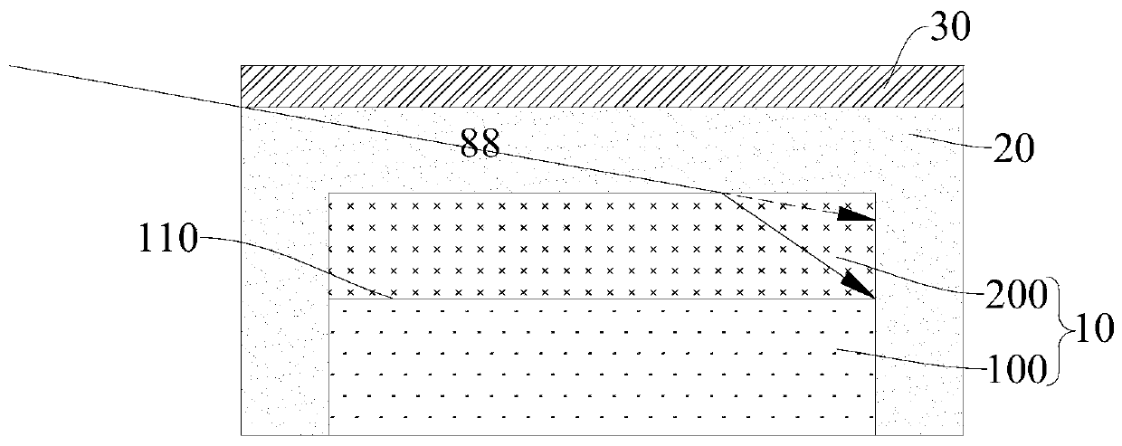
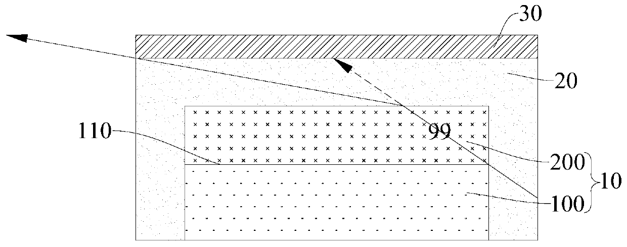
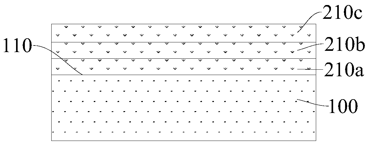
[0030] In one aspect of the present invention, the present invention provides a fingerprint recognition module for a liquid crystal display panel. According to an embodiment of the present invention, refer to figure 1 and figure 2 , the fingerprint identification module 10 includes: an optical fingerprint identification sensor 100; an insulating layer 200, the insulating layer 200 is arranged on the ph...


PUM


Abstract

The invention provides a fingerprint identification module for a liquid crystal display panel, an array substrate, a manufacturing method of the array substrate and the liquid crystal display panel. The fingerprint identification module comprises an optical fingerprint identification sensor; and an insulating layer, wherein the insulating layer is arranged on the photosensitive surface of the optical fingerprint identification sensor, the insulating layer is in contact with the liquid crystal in the liquid crystal display panel, and the refractive index of the insulating layer is greater thanthe abnormal refractive index of the liquid crystal. When the fingerprint identification module is used in the liquid crystal display panel, more light reflected at the finger pressing position can beemitted into the optical fingerprint identification sensor, so that the utilization rate of reflected light during fingerprint identification is high, the detection precision of the optical fingerprint identification sensor is high, and the fingerprint identification function is well achieved; meanwhile, the direction of light emitted from the liquid crystal display panel is changed, so that thelight which should be emitted into the black matrix is emitted out of the liquid crystal display panel, the transmittance of the liquid crystal display panel is high, and a display picture is good.

Description

technical field [0001] The invention relates to the field of display technology, in particular to a fingerprint recognition module, an array substrate and a manufacturing method thereof, and a liquid crystal display panel. Background technique [0002] In related technologies, the optical fingerprint recognition technology realizes fingerprint recognition by identifying the difference in the intensity of light reflected by the finger into the optical fingerprint recognition sensor due to the different reflectivity of the ridges or valleys on the surface of the finger after the light is irradiated on the finger. identify. However, when it is directly applied to the liquid crystal display panel, due to the low light transmittance of the backlight module, most of the light reflected by the finger cannot enter the optical fingerprint recognition sensor, so the fingerprint recognition cannot be well realized. function. [0003] Therefore, the related technology of fingerprint i...

Claims


Application Information

Patent Timeline
IPC IPC(8): G06K9/00G02F1/1333G02F1/1362G02F1/1368
CPCG02F1/13338G02F1/136286G02F1/1368G06V40/1318
Inventor 张慧
Owner BOE TECH GRP CO LTD
Why Eureka
Try Eureka