Frequency response test device and method of all-in-one photoelectric device

A technology of frequency response testing and optoelectronic devices, which is applied in the field of optoelectronics, can solve the problems that the spectral analysis method cannot realize the frequency response test of photodetectors, low frequency resolution of measurement, complicated process, etc., and achieve the realization of frequency response testing of optoelectronic devices, Test the effect of simple structure and low cost

Active Publication Date: 2019-08-30
CHONGQING UNIV OF POSTS & TELECOMM
View PDF12 Cites 21 Cited by
  • Summary
  • Abstract
  • Description
  • Claims
  • Application Information

AI Technical Summary

Problems solved by technology

Among them, in the optical domain test method, the spectral analysis method can realize the measurement of the frequency response of the electro-optic modulator, (Y.Q.Shi, L.S.Yan, A.E.Willner, "High-speed electrooptic modulator characterization using optical spectrum analysis," Journal of Lightwave Technology, 2003, 21(10):2358-2367), however, the measurement accuracy of this scheme depends heavily on the resolution of the spectrum analyzer, and there are usually problems of low measurement frequency resolution and low precision. In addition, the spectral analysis method cannot realize the photodetector Frequency response test; in the electrical domain measurement method, the frequency sweep method (Y.Q.Heng, M.Xue, W.Chen, S.L.Han, J.Q.Liu, and S.L.Pan, “Large-dynamic frequency frequency measurement for broadband electro-optic phase modulators , "IEEE Photonics Technology Letters, 2019, 31(4): 291-294. D.A. Humphreys, "Integrated-optic system for high-speed photodetector bandwidth measurements," Electronics Letters, 1989, 25(23): 1555-1557.) fully Utilizing the high-precision test characteristics of vector network analyzers, high-precision relative frequency response testing of optoelectronic devices can be achieved. However, additional calibration is required and the process is complicated; the frequency-shifting heterodyne method (S.J.Zhang, C.Zhang, H.Wang , X.H.Zou, Y.L.Zhang, Y.Liu, and J.E.Bowers, "Self-calibrated microwave characterization of high-speed optoelectronic devices by heterodyne spectrum mapping," Journal of Lightwave Technology, 35(10), 1952-1961.) is using heterodyne The principle of interference, by configuring the frequency relationship of two modulation signals, achieves high-precision, self-calibrating absolute frequency response testing of optoelectronic devices. However, this solution requires an additional auxiliary broadband microwave source and broadband modulator to eliminate other components in the system. The influence of frequency response, the system pin big

Method used


Image

  • Frequency response test device and method of all-in-one photoelectric device
  • Frequency response test device and method of all-in-one photoelectric device
  • Frequency response test device and method of all-in-one photoelectric device

Examples


Embodiment

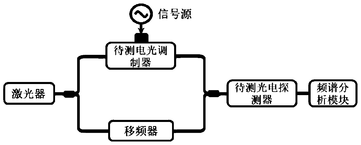
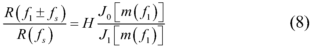
[0072] Laser output power is 10mW, frequency f 0 = 193THz (wavelength about 1550nm) optical carrier. The frequency of the microwave signal source is f 1 = 20GHz sinusoidal signal to modulate the electro-optical modulator to be tested. In the lower arm of the frequency-shifted heterodyne interference module, the frequency shift of the optical carrier is 70MHz. The coupled output signals of the upper and lower arms are detected by the photodetector to be tested, and the output light The current is analyzed through the spectrum analysis module, and the powers driven by two different signals are 10dBm and 4dBm respectively. At this time, the voltage amplitude ratio of the driving signals is r=0.5. (1) During the phase modulator and photodetector frequency response test, the amplitude ratios of the mixed frequency signals driven by two different signals are H=-16.52dB and H'=-22.65dB respectively, then the ratio of the two amplitude ratios is 6.14dB, obtained by the formula (7), ...


PUM


Abstract

The invention requests and protects a frequency response test device and method of an all-in-one photoelectric device. The frequency response test device comprises a laser, a frequency-shift heterodyne interference module, a to-be-measured detector and a spectral analysis module, wherein the frequency-shift heterodyne interference module comprises a to-be-measured photoelectric modulator and a frequency shifter which are respectively placed in an Mach-Zehnder arm and a lower Mach-Zehnder arm of an interference module, the laser, the frequency-shift heterodyne interference module and the to-be-measured photoelectric detector are sequentially and optically connected, a microwave signal source is electrically connected with an input electrode end of the to-be-measured photoelectric modulator,and an output end of the to-be-measured photoelectric modulator is electrically connected with the spectral analysis module. A power ratio of a corresponding constituent is obtained by the spectral analysis module under the condition that the microwave signal source is driven by two different output voltages under the same working frequency, frequency response test of the to-be-measured photoelectric modulator is achieved, the frequency response of the to-be-measured photoelectric modulator is further inversely calculated, and automatic calibration test of the frequency response is finally achieved.

Description

technical field [0001] The invention belongs to the technical field of optoelectronics, and in particular relates to an all-in-one optoelectronic device frequency response testing device and method. Background technique [0002] With the advent of 5G mobile communication, people's demand for communication speed and data capacity has shown explosive growth. At present, the rapid development of optical fiber communication system is the basic guarantee for the promotion of 5G mobile communication in the future. As a basic component of optical fiber communication system - optoelectronic devices, its characteristic parameters are the key to determine the communication capacity, bandwidth and speed. At the same time, the realization of optoelectronic Accurate characterization of device characteristic parameters plays a vital role in the development, design, manufacture and optimization of optoelectronic devices, so the study of optoelectronic device characteristic parameters is pa...

Claims


Application Information

Patent Timeline
Patent Type & Authority Applications(China)
IPC IPC(8): G01R23/17G01M11/02
CPCG01M11/0292G01R23/17
Inventor 邹新海亓林刘宇路永乐郭俊启黎人溥邸克崔巍文丹丹
Owner CHONGQING UNIV OF POSTS & TELECOMM
Why Eureka
Try Eureka