POD digital printing technology based on IOT (Internet of Things) technology
An Internet of Things technology and digital printing technology, which is applied in the field of POD digital printing technology, can solve the problems of reducing production efficiency, being unable to control, and not being able to deal with it in the first time, so as to reduce maintenance time and improve production efficiency.
- Summary
- Abstract
- Description
- Claims
- Application Information
AI Technical Summary
Problems solved by technology
Method used
Image
Examples
Embodiment 1
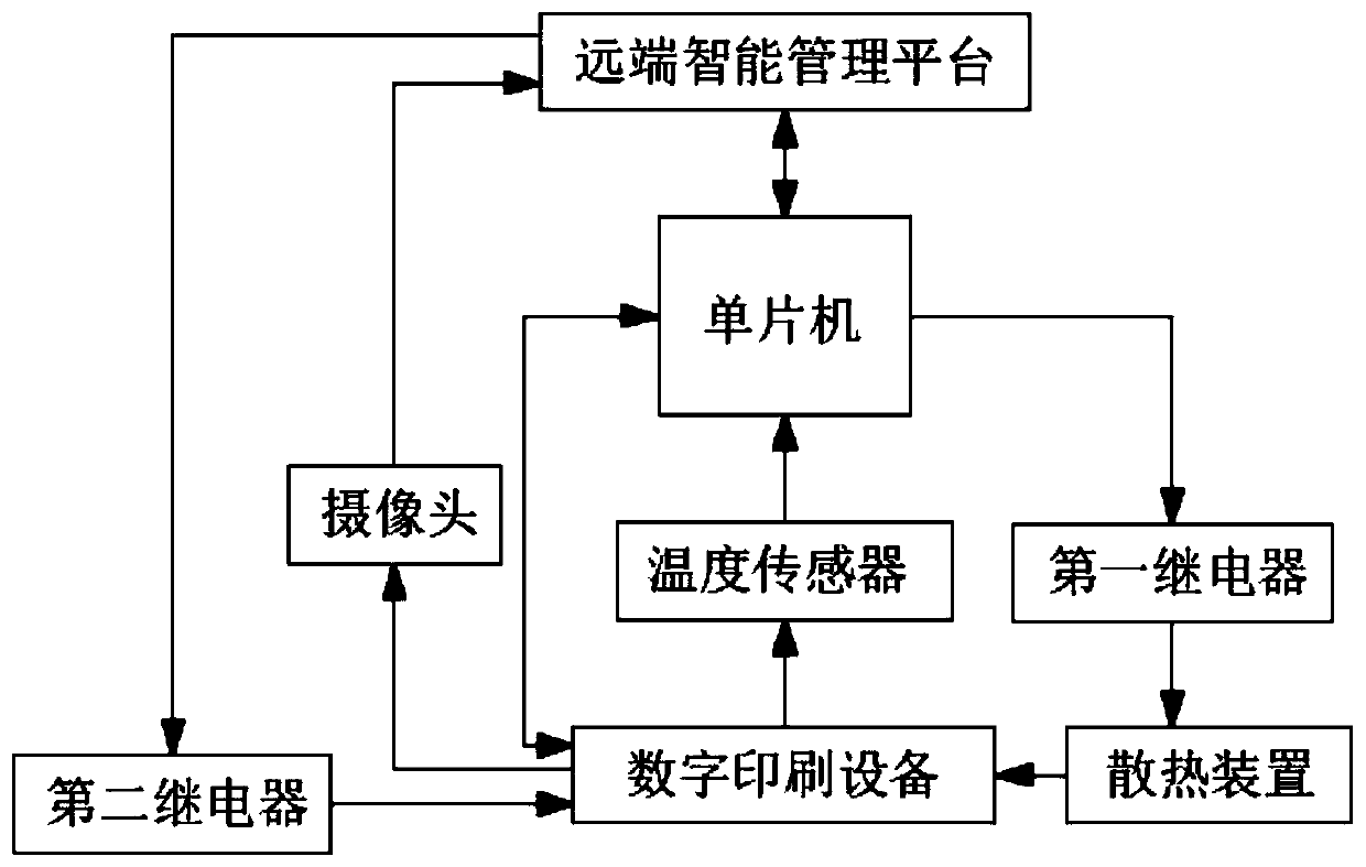
[0024] see Figure 1-3 , a POD digital printing process based on Internet of Things technology, the POD digital printing process based on Internet of Things technology is as follows:
[0025] Step 1: Connect the digital printing equipment to the remote intelligent management platform with the support of the network, and know the operating status of the equipment in real time at the remote end, so as to prevent the occurrence of failures in advance, and add a camera to the digital printing equipment to monitor the printing equipment. Carry out real-time monitoring. When the equipment fails, the remote intelligent management platform directly sends a signal to the second relay, and the second relay controls the circuit disconnection of the digital printing equipment, so that it can be found and processed at the first time;
[0026] Step 2: Install a temperature sensor inside the digital printing equipment. The temperature sensor is connected to the single-chip microcomputer. The...
Embodiment 2
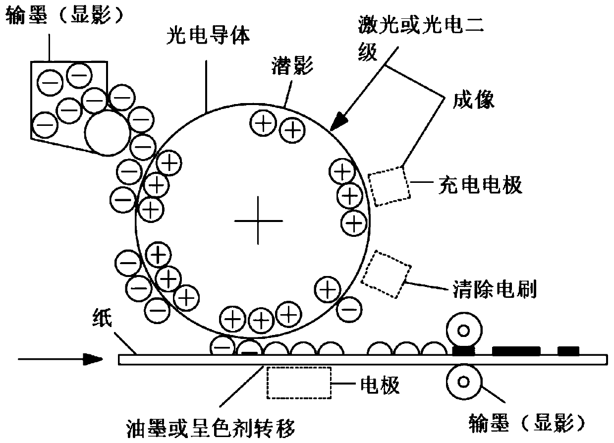
[0030] Please focus on image 3 , digital printing equipment adopts electrophotographic imaging, and the steps are as follows:
[0031] Step 1: First charge the surface of the photoconductive drum to form a uniform layer of charge, then the surface of the photoconductive drum is imaged under the action of light, and the charge on the exposed area of the photoconductive drum surface is released to form a non-graphic area, and the unexposed part of the charge Retention, so that a "charge image" is formed on the photoconductive drum, that is, a "latent image";
[0032] Step 2: Under the action of the electric field force, the latent image area on the surface of the photoconductive drum absorbs ink or colorant to form a visible image, which is the so-called "development";
[0033] Step 3: Relying on the electric field force of the electrode to the charged ink or coloring agent, the ink or coloring agent on the surface of the photoconductive drum is directly transferred to the s...
Embodiment 3
[0037] Please focus on image 3 1. After the ink or coloring agent on the surface of the photoconductive drum is transferred to the substrate, the ink or coloring agent on the surface of the photoconductive drum is mechanically removed, and at the same time, electronic cleaning and processing are also performed.
[0038] The ink or coloring agent on the surface of the photoconductive drum in this embodiment is not completely transferred to the substrate, and a part remains on the surface of the conductive drum. The agent is mechanically removed, and at the same time, it is electronically removed and treated to return the photoconductive drum surface to a neutral state.
PUM
 Abstract
Description
Claims
Application Information
 - R&D
- Intellectual Property
- Life Sciences
- Materials
- Tech Scout
- Unparalleled Data Quality
- Higher Quality Content
- 60% Fewer Hallucinations
Browse by: Latest US Patents, China's latest patents, Technical Efficacy Thesaurus, Application Domain, Technology Topic, Popular Technical Reports.
© 2025 PatSnap. All rights reserved.Legal|Privacy policy|Modern Slavery Act Transparency Statement|Sitemap|About US| Contact US: help@patsnap.com


