Supercharge Your Innovation With Domain-Expert AI Agents!

An on-chip dense waveguide-based nanoparticle sensor and its sensing method

A nanoparticle and sensing method technology, applied in the direction of instruments, scientific instruments, measuring devices, etc., can solve the problems of small sensing area, photodestruction of biomolecules, long-term capture of nanoparticles, etc., to achieve large sensing area, The effect of fast time response and high capture efficiency

Active Publication Date: 2020-10-09
PEKING UNIV
View PDF5 Cites 0 Cited by
  • Summary
  • Abstract
  • Description
  • Claims
  • Application Information

AI Technical Summary

Problems solved by technology

Although the sensitivity of these sensors has exceeded the requirements of current applications, the following aspects seriously hinder the promotion of their practical applications: 1. The sensing area of ​​the micro-nano scale resonant cavity is extremely small, so it takes a very long time to capture and characterize nanoparticles
Although nanofiber coils and arrays can increase the detection area, the low axial uniformity of nanofibers, difficulty in integrating with microfluidics, and associated nanofiber fixtures limit the practical application of such sensors.
2. High power densities in microcavities and plasmonic resonators can have photodestructive effects on biomolecules
3. The preparation process of optical sensors such as nanofibers, microcavities and semi-continuous plasmonic films is difficult to achieve precise control, resulting in inconsistent performance of the prepared sensors

Method used


Image

  • An on-chip dense waveguide-based nanoparticle sensor and its sensing method
  • An on-chip dense waveguide-based nanoparticle sensor and its sensing method
  • An on-chip dense waveguide-based nanoparticle sensor and its sensing method

Examples


Embodiment Construction

[0041] Below in conjunction with the accompanying drawings, the present invention will be further described through specific embodiments.

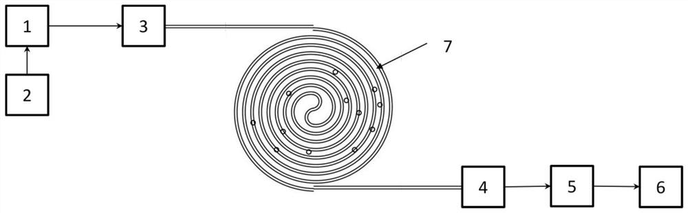
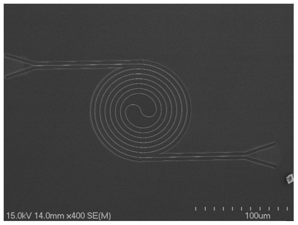
[0042] like figure 1 As shown, the nanoparticle sensor based on the on-chip dense waveguide of this embodiment includes: a substrate, a single waveguide, a light source device, first and second fiber optic waveguide couplers 3 and 4, a photodetector 5, a data acquisition card 6 and Computer; wherein, the light source device includes a laser 1 and a function generator 2; a single waveguide is wound on the surface of the substrate at the maximum density level under certain conditions, and the radius of curvature of the shape formed by winding is greater than 5 μm to reduce the loss of light, thereby on the substrate The dense waveguide 7 is formed on the surface of the surface; the first fiber waveguide coupler 3 is set at one end of the single waveguide, and the second fiber waveguide coupler 4 is set at the other end of the single waveguid...


PUM

PropertyMeasurementUnit
radiusaaaaaaaaaa

Abstract

The invention discloses an on-chip intensive waveguide-based nanoparticle sensor and a sensing method thereof. A single waveguide is horizontally wound around a surface of a substrate to form an intensive waveguide with maximum density under a condition that coupling is not generated, detection light is scattered or absorbed by nanoparticles when the nanoparticles attached onto a surface of the intensive waveguide are arranged within an evanescent field of a waveguide mode, an abruptly-descending step signal is generated by transmitting power, the size information of the nanoparticle is codedby the step signal, whether the nanoparticle exists or not is judged through identifying the step signal by a computer, and the size information of the nanoparticle is obtained. The intensive waveguide is large in sensing area, and the sensing area is expanded than that of a straight waveguide by two orders of magnitude; meanwhile, the capturing efficiency is high, and the time response is rapid,and the nanoparticle small sphere with radius being 100 nanometers can be detected; and moreover, the scattering signal of the waveguide mode of TM polarization is 30 times of that of TE polarization.

Description

technical field [0001] The invention relates to nanoparticle sensing technology, in particular to a nanoparticle sensor based on an on-chip dense waveguide and a sensing method thereof. Background technique [0002] At present, related fields such as homeland security, environmental monitoring, and early diagnosis are in urgent need of in-situ, rapid, ultra-sensitive, and reproducible detection platforms for nanoscale particles. Among various sensors, optical evanescent field sensors have attracted more and more attention due to many unique advantages, such as high sensitivity, no labeling, and non-invasiveness. In recent years, related studies have mainly focused on exploring new mechanisms to enhance the sensitivity of sensors. For example, the use of singular points in the microcavity or the combination of plasmon enhancement effect can improve the sensitivity of the sensor to the detection of single biomolecules and single atoms. Nanofibers exploit the concept of photo...

Claims


Application Information

Patent Timeline
Patent Type & Authority Patents(China)
IPC IPC(8): G01N21/84G01N21/01G01B11/00G01V8/16
CPCG01B11/00G01N21/01G01N21/84G01N2021/0112G01N2021/8472G01N2201/08G01V8/16
Inventor 肖云峰唐水晶俞骁翀龚旗煌
Owner PEKING UNIV
Features
  • R&D
  • Intellectual Property
  • Life Sciences
  • Materials
  • Tech Scout
  • Unparalleled Data Quality
  • Higher Quality Content
  • 60% Fewer Hallucinations
Learn More