Array substrate, liquid crystal display panel and liquid crystal display device
An array substrate and array arrangement technology, which is applied in instruments, nonlinear optics, optics, etc., can solve the problems of low brightness in black state, poor contrast, poor display, etc.
- Summary
- Abstract
- Description
- Claims
- Application Information
AI Technical Summary
Problems solved by technology
Method used
Image

Examples
Embodiment 1
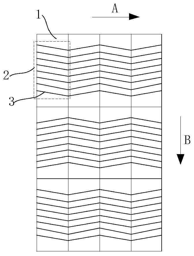
[0034] An array substrate is provided in Embodiment 1, refer to figure 1 As shown, the array substrate in the first embodiment includes a plurality of sub-pixels 1 arranged in an array, and each sub-pixel 1 includes a pixel electrode, wherein each pixel electrode includes a domain-oriented electrode region 2, that is, The pixels of the array substrate are designed in a single-domain pixel mode, wherein, along the row direction, the domain directions in the electrode region 2 of every two adjacent pixel electrodes are different from each other; along the column direction, every two adjacent pixel electrodes have The domain orientations in the electrode regions 2 of the electrodes are different from each other.
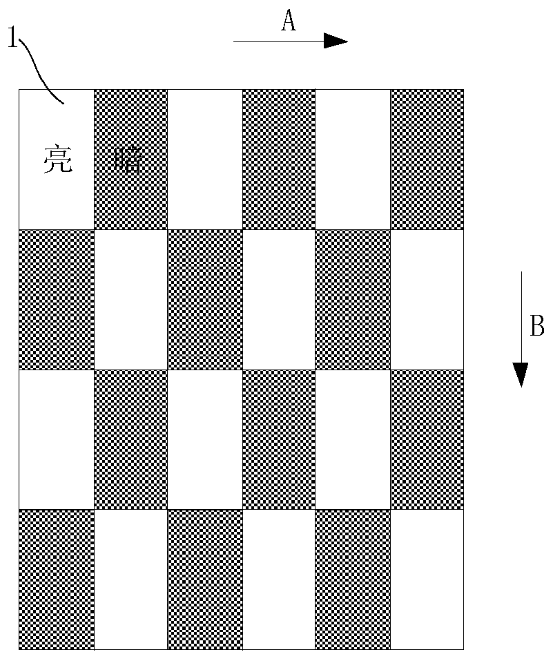
[0035] In the array substrate of the first embodiment above, in the row direction and the column direction, the domain directions of the electrode regions 2 in every two adjacent pixel electrodes are different, according to figure 1 combine image 3 As shown, when the...
Embodiment 2
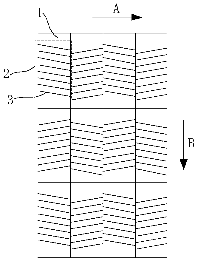
[0049] An array substrate is provided in the second embodiment, refer to Figure 5 As shown, the array substrate in the second embodiment includes a plurality of sub-pixels 1 arranged in an array, and each sub-pixel 1 includes a pixel electrode, wherein each pixel electrode includes two The electrode regions 2 that are different from each other, that is, the pixel in the second embodiment is designed as a double-chip pixel mode, wherein, along the row direction, in every two adjacent pixel electrodes, the domain directions in the adjacent electrode regions 2 are not mutually same; along the column direction, in every two adjacent pixel electrodes, the domain directions in the adjacent electrode regions 2 are different from each other.
[0050] In the array substrate in the second embodiment above, in the row direction and the column direction, in every two adjacent pixel electrodes, the domain directions of the adjacent electrode regions 2 are different, according to Figure ...
PUM
| Property | Measurement | Unit |
|---|---|---|
| angle | aaaaa | aaaaa |
Abstract
Description
Claims
Application Information
 - R&D
- Intellectual Property
- Life Sciences
- Materials
- Tech Scout
- Unparalleled Data Quality
- Higher Quality Content
- 60% Fewer Hallucinations
Browse by: Latest US Patents, China's latest patents, Technical Efficacy Thesaurus, Application Domain, Technology Topic, Popular Technical Reports.
© 2025 PatSnap. All rights reserved.Legal|Privacy policy|Modern Slavery Act Transparency Statement|Sitemap|About US| Contact US: help@patsnap.com