Micro capillary electrophoresis chip and preparation method thereof

A microcapillary, electrophoresis chip technology, applied in chemical instruments and methods, material analysis by electromagnetic means, laboratory containers, etc. Reduce inspection cost and improve integration effect

Active Publication Date: 2022-01-04
重庆高开清芯科技产业发展有限公司
View PDF4 Cites 0 Cited by
  • Summary
  • Abstract
  • Description
  • Claims
  • Application Information

AI Technical Summary

Problems solved by technology

The cost of most optical devices is very high, tens of thousands or even millions, which limits the popularity of microfluidic chips in households and small hospitals and clinics

Method used


Image

  • Micro capillary electrophoresis chip and preparation method thereof
  • Micro capillary electrophoresis chip and preparation method thereof
  • Micro capillary electrophoresis chip and preparation method thereof

Examples


Embodiment 1

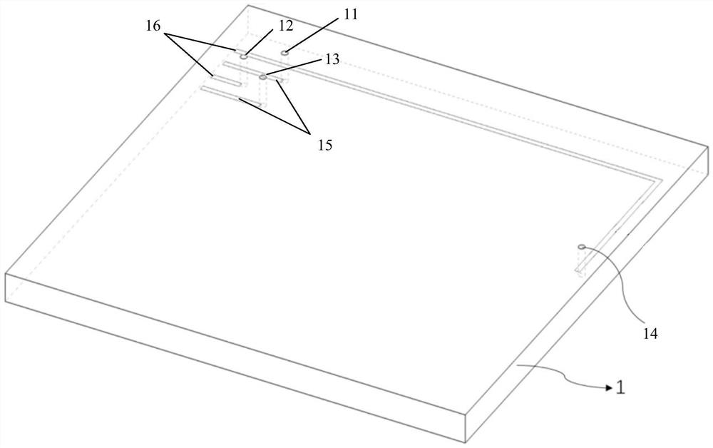
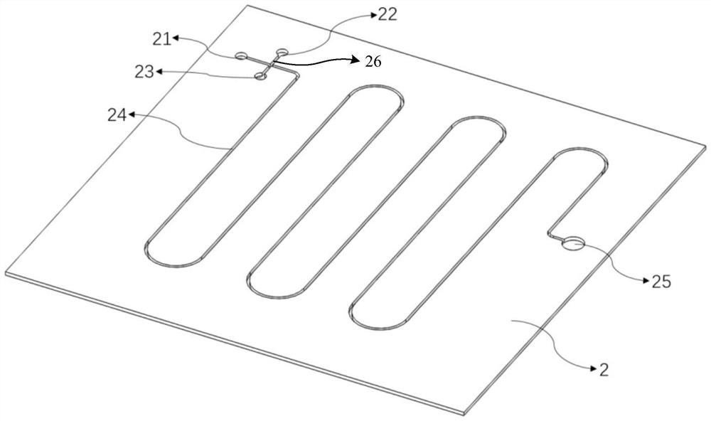
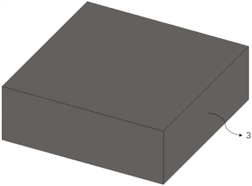
[0050] Such as figure 1 A schematic diagram of the structure of the first layer of the microcapillary electrophoresis chip in one embodiment shown, figure 2 A schematic diagram of the second layer structure of the microcapillary electrophoresis chip in one embodiment of the present invention is shown, image 3 A schematic diagram of the third layer structure of the microcapillary electrophoresis chip in one embodiment of the present invention is shown, Figure 4 Shown is a schematic diagram of the bonding of the first layer structure, the second layer structure and the third layer structure of the microcapillary electrophoresis chip in one embodiment of the present invention.

[0051] combine Figure 1 to Figure 4 As shown, according to an embodiment of the present invention, a microcapillary electrophoresis chip includes a first layer structure 1, at least one group of micro metal electrodes is arranged on the lower surface of the first layer structure, and at least one liqu...

Embodiment 2

[0078] The difference between this embodiment and the first embodiment is that the silicon chip of the CMOS CMOS detection circuit of the CMOS image sensor is processed on the surface to form micro-channels.

[0079] According to an embodiment of the present invention, a microcapillary electrophoresis chip includes a first layer structure, at least one group of micro metal electrodes is arranged on the lower surface of the first layer structure, and at least one liquid inlet hole and one liquid outlet are opened through the first layer structure hole.

[0080] In some embodiments, a first liquid inlet hole and a second liquid inlet hole are opened through the first layer structure, and a first liquid outlet hole and a second liquid outlet hole are opened through the first layer structure. The first group of micro metal electrodes and the second group of micro metal electrodes are arranged on the lower surface of the first layer structure.

[0081] According to an embodiment o...


PUM


Abstract

The present invention provides a micro capillary electrophoresis chip comprising a first layer structure, at least one group of micro metal electrodes are arranged on the lower surface of the first layer structure, and at least one liquid inlet hole and one liquid outlet hole are opened through the first layer structure; the second A layer structure, etching microchannels on the surface of the second layer structure, and a liquid storage chamber, a buffer chamber, a first waste liquid chamber and a second waste liquid chamber; a third layer structure, the third layer structure is CMOS A detection circuit layer, the upper surface of the CMOS detection circuit is a silicon chip; the first layer structure is bonded to the second layer structure, so that the liquid inlet hole is aligned with the liquid storage cavity or buffer cavity, and the The liquid outlet hole is aligned with the first waste liquid chamber or the second waste liquid chamber, and the second layer structure is bonded to the silicon chip on the upper surface of the CMOS detection circuit. The chip structure of the present invention is highly integrated, the traditional electrophoresis chip detection device is simplified, the detection cost is reduced, and fast on-chip detection is realized.

Description

technical field [0001] The invention relates to the technical field of electrophoresis chips, in particular to a microcapillary electrophoresis chip and a preparation method thereof. Background technique [0002] In recent years, microfluidic chip technology has attracted widespread attention due to its advantages of high integration, low material consumption, fast detection speed, and low cost. In the laboratory field, microfluidic chip technology has been relatively mature in many biomedical fields, such as DNA extraction and detection, cell separation, drug analysis, etc. [0003] However, the main difficulty restricting the development of microfluidic chips towards industrialization is the packaging technology and detection technology of microfluidic chips. For the packaging of microfluidic chips, although the packaging methods of microfluidic chips with different functions may be different, the packaging methods for specific chips are often the same. As for the detect...

Claims


Application Information

Patent Timeline
Patent Type & Authority Patents(China)
IPC IPC(8): G01N27/447B01L3/00G01N21/84
CPCG01N27/44791B01L3/5027G01N21/84
Inventor 林孝康张明哲傅嵩
Owner 重庆高开清芯科技产业发展有限公司
Why Eureka
Try Eureka