

Photographing optical lens system, image capturing unit and electronic device
一种光学镜头、透镜的技术,应用在摄像用光学镜头,取像装置及电子装置领域
- Summary
- Abstract
- Description
- Claims
- Application Information
AI Technical Summary
Problems solved by technology
Method used
Image

Examples
no. 1 example
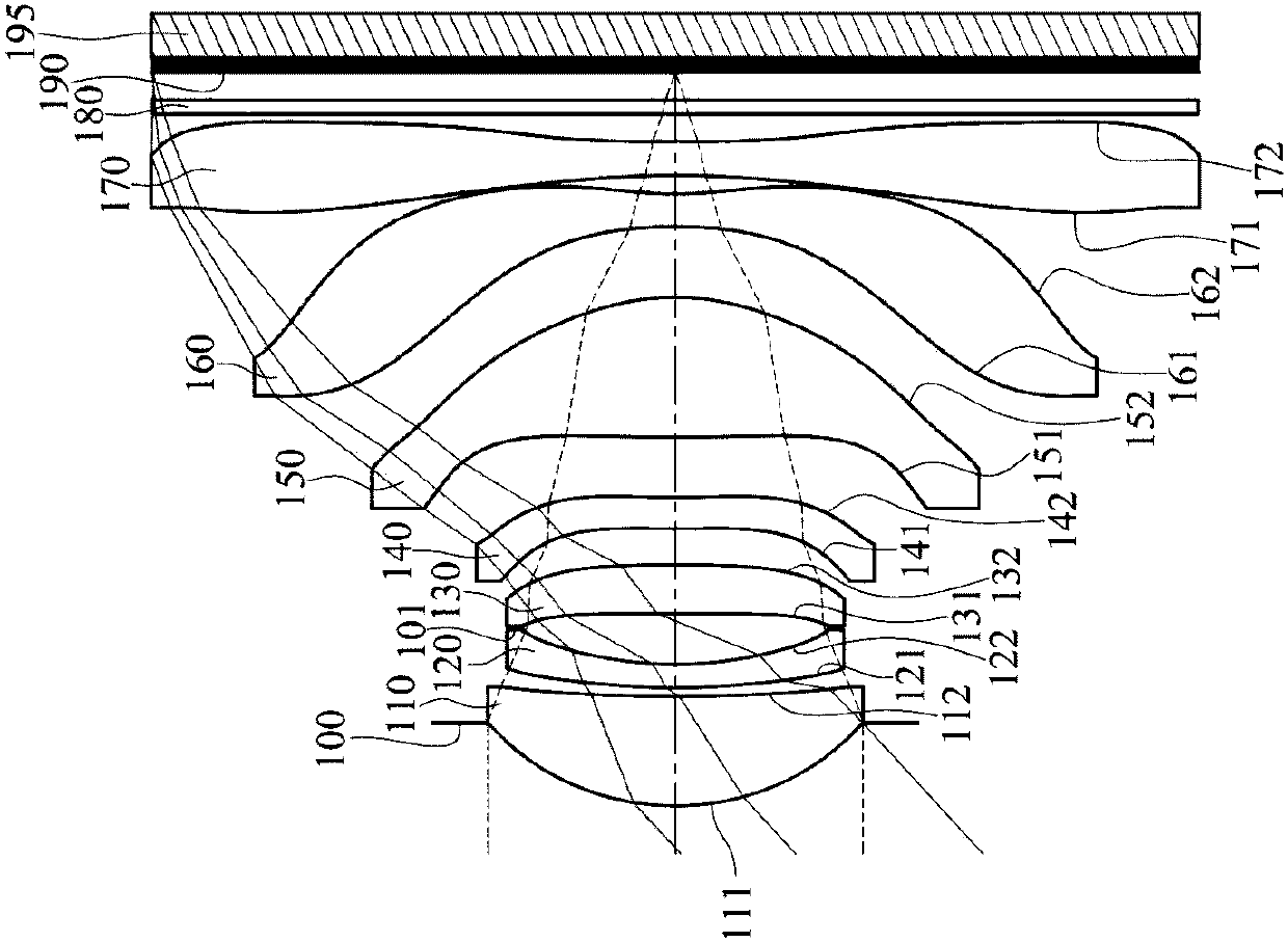
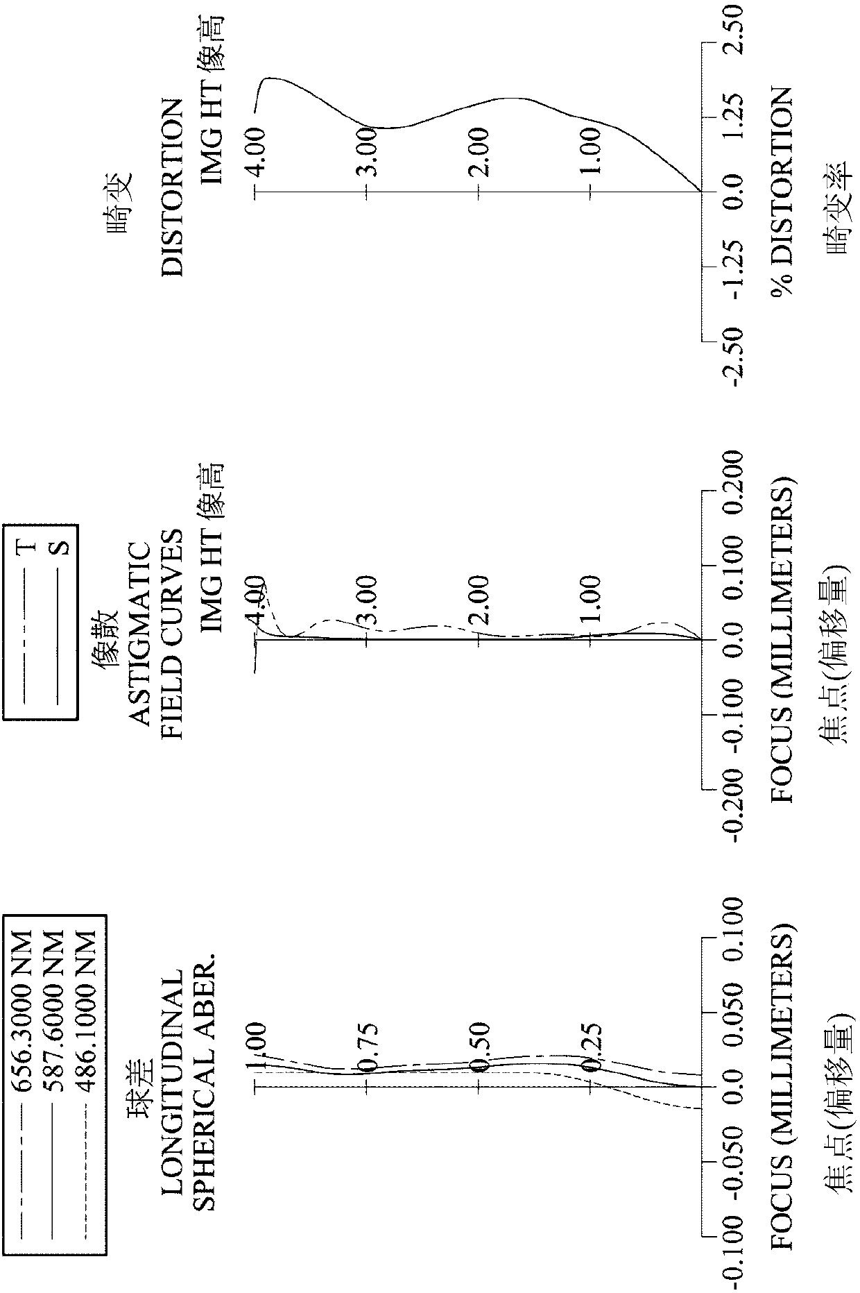
[0139] Please refer to Figure 1 to Figure 2 ,in figure 1 A schematic diagram of an imaging device according to a first embodiment of the present invention is shown, figure 2 From left to right are the spherical aberration, astigmatism and distortion curves of the first embodiment. Depend on figure 1 It can be seen that the image capturing device includes an optical lens for imaging (not another number) and an electronic photosensitive element 195 . The optical lens for imaging includes an aperture 100, a first lens 110, a second lens 120, a diaphragm 101, a third lens 130, a fourth lens 140, a fifth lens 150, a sixth lens 160, The seventh lens 170 , the filter element (Filter) 180 and the imaging surface 190 . Wherein, the electronic photosensitive element 195 is disposed on the imaging surface 190 . The optical lens for imaging includes seven single non-cemented lenses (110, 120, 130, 140, 150, 160, 170), and there is no interpolated lens between each lens. Wherein, t...
no. 2 example
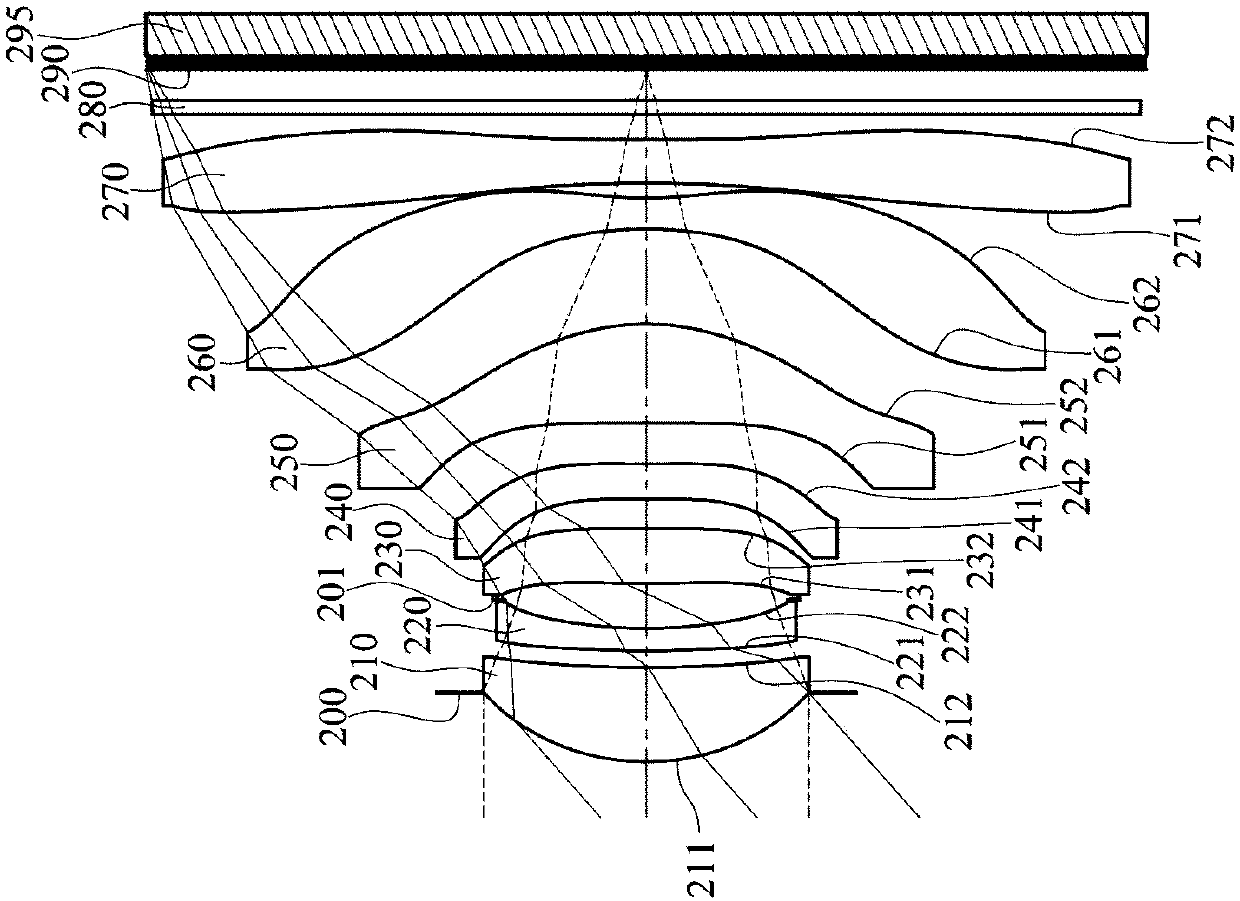
[0180] Please refer to Figure 3 to Figure 4 ,in image 3 A schematic diagram of an imaging device according to a second embodiment of the present invention is shown, Figure 4 From left to right are the spherical aberration, astigmatism and distortion curves of the second embodiment. Depend on image 3 It can be seen that the image capturing device includes an optical lens for imaging (not another number) and an electronic photosensitive element 295 . The optical lens for imaging includes an aperture 200, a first lens 210, a second lens 220, a diaphragm 201, a third lens 230, a fourth lens 240, a fifth lens 250, a sixth lens 260, The seventh lens 270 , the filter element 280 and the imaging surface 290 . Wherein, the electronic photosensitive element 295 is disposed on the imaging surface 290 . The optical lens for imaging includes seven single non-cemented lenses (210, 220, 230, 240, 250, 260, 270), and there is no interpolated lens between each lens. Wherein, there is...
no. 3 example
[0197] Please refer to Figure 5 to Figure 6 ,in Figure 5 A schematic diagram of an imaging device according to a third embodiment of the present invention is shown, Figure 6 From left to right are the spherical aberration, astigmatism and distortion curves of the third embodiment. Depend on Figure 5 It can be seen that the image capturing device includes an optical lens for imaging (not another number) and an electronic photosensitive element 395 . The optical lens for imaging includes a diaphragm 300, a first lens 310, a second lens 320, a third lens 330, a fourth lens 340, a fifth lens 350, a sixth lens 360, and a seventh lens 370 from the object side to the image side. , the filter element 380 and the imaging surface 390 . Wherein, the electronic photosensitive element 395 is disposed on the imaging surface 390 . The optical lens for imaging includes seven single non-cemented lenses (310, 320, 330, 340, 350, 360, 370), and there is no interpolated lens between each...
PUM
 Abstract
Description
Claims
Application Information