Ultra-broadband perfect absorber in mid-infrared band and preparation method thereof
An infrared band and ultra-broadband technology, applied in the field of wave absorbers, can solve the problems of narrow operating band, poor thermal stability, and low absorption efficiency of broadband absorbers, and achieve saving manpower and material resources, good thermal stability, and high absorption efficiency Effect
- Summary
- Abstract
- Description
- Claims
- Application Information
AI Technical Summary
Problems solved by technology
Method used
Image

Examples
preparation example Construction
[0036] The preparation method of the above-mentioned ultra-broadband perfect absorber in the mid-infrared band, comprising the following steps:
[0037] Step 1. Prepare clean glass pieces;
[0038] Step 2, coating, a layer of metal film is evaporated on the glass sheet in step 1 to form a base layer 1;
[0039] Step 3, coating, a layer of semiconductor material is evaporated on the base layer 1 in step 2 to form a non-metallic dielectric layer 2;
[0040] Step 4, laying metal nanostructures, and laying metal nanostructures on the non-metallic dielectric layer 2 in step 3 to form a metal absorption layer 3;
[0041] Step 5: Coating, vapor-depositing a layer of semiconductor material on the metal absorption layer 3 in Step 4 to form a top non-metallic anti-reflection layer 4 to obtain an ultra-broadband perfect absorber in the mid-infrared band.
[0042] In step 4, the inverse structure of the target structure is formed by spin coating photoresist on the surface of the non-met...
Embodiment 1
[0044] A kind of ultra-broadband perfect absorber in the mid-infrared band of the present embodiment is as follows:
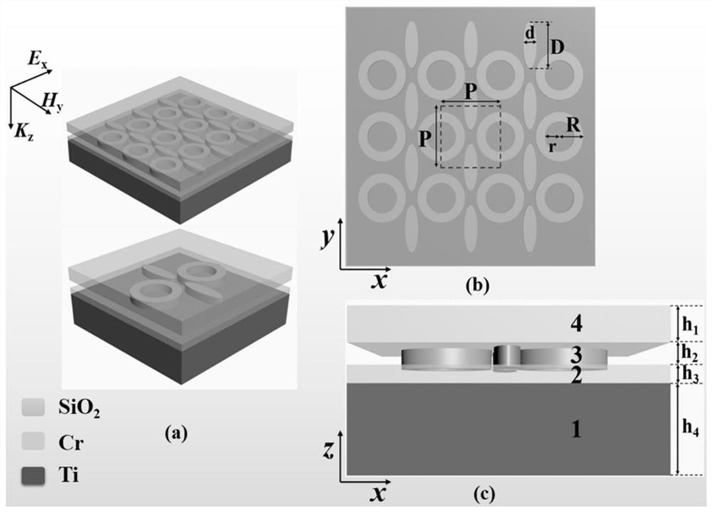
[0045] Base layer 1, material is titanium, thickness h 3 = 300 nm;
[0046] Non-metallic dielectric layer 2, material is silicon dioxide, thickness h 2 = 50 nm;
[0047] Metal absorption layer 3, material is chromium, thickness h 1 = 70 nm;
[0048] Non-metallic anti-reflection layer 4, material is silicon dioxide, thickness h 4 = 200 nm;
[0049] Among them, the metal absorption layer 3 is formed by a periodic array of two nano-rings and two elliptical nano-disks, and the array period (P) is 400 nanometers; the outer radius (R) of the nano-ring is 160 nanometers, and the inner radius (r ) is 50 nm; the major semi-axis (D) of the elliptical nanodisk is 150 nm, and the minor semi-axis (d) is 60 nm.
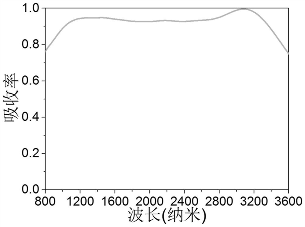
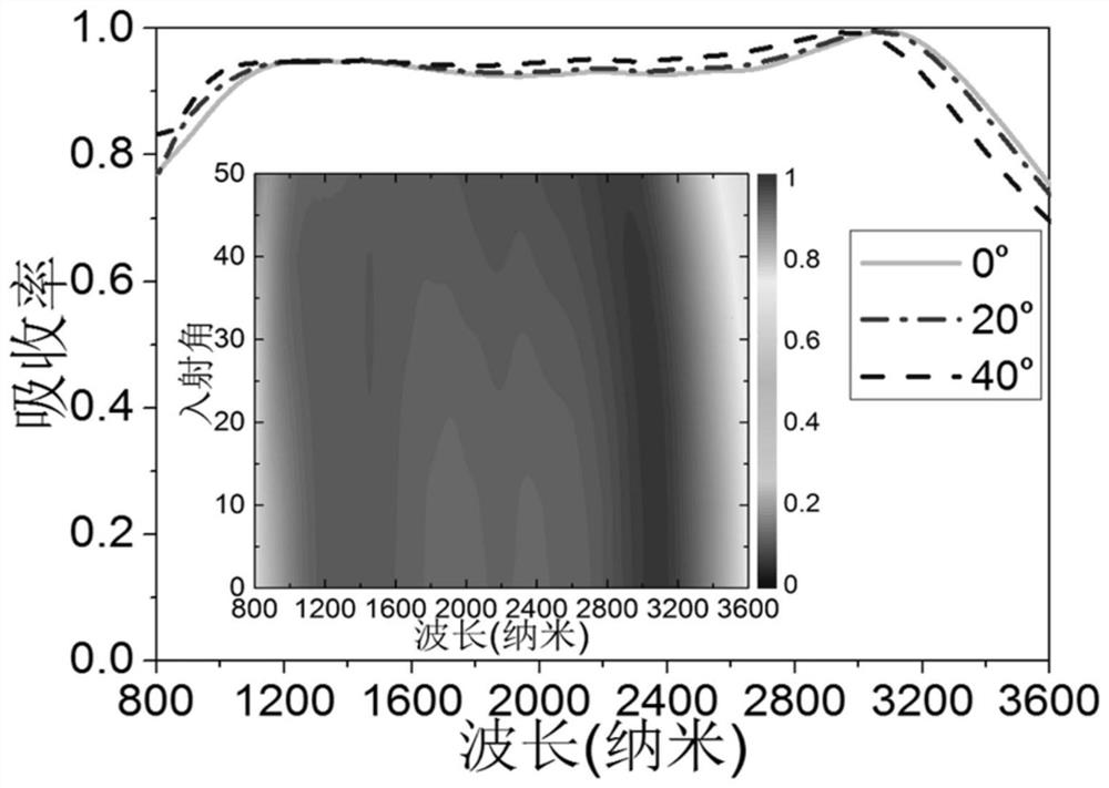
[0050] figure 2 The absorption spectrum of the ultra-broadband perfect absorber in the infrared band in this example is shown. It can be clearly seen that ...
Embodiment 2
[0053] On the basis of Example 1, the non-metallic anti-reflection layer 4 is removed, and the others are the same as Example 1. That is, the thickness of the non-metallic anti-reflection layer 4 is 0 nm.
PUM
| Property | Measurement | Unit |
|---|---|---|
| thickness | aaaaa | aaaaa |
| thickness | aaaaa | aaaaa |
| thickness | aaaaa | aaaaa |
Abstract
Description
Claims
Application Information
 - R&D
- Intellectual Property
- Life Sciences
- Materials
- Tech Scout
- Unparalleled Data Quality
- Higher Quality Content
- 60% Fewer Hallucinations
Browse by: Latest US Patents, China's latest patents, Technical Efficacy Thesaurus, Application Domain, Technology Topic, Popular Technical Reports.
© 2025 PatSnap. All rights reserved.Legal|Privacy policy|Modern Slavery Act Transparency Statement|Sitemap|About US| Contact US: help@patsnap.com