PCB conveying device
A technology for PCB boards and transportation devices, applied in the field of PCB board manufacturing, can solve problems such as easy jamming and easy damage of PCB boards, and achieve the effects of avoiding offset, improving yield, and avoiding relative sliding.
- Summary
- Abstract
- Description
- Claims
- Application Information
AI Technical Summary
Problems solved by technology
Method used
Image

Examples
Embodiment Construction
[0025] Now in conjunction with the accompanying drawings, the preferred embodiments of the present invention will be described in detail.
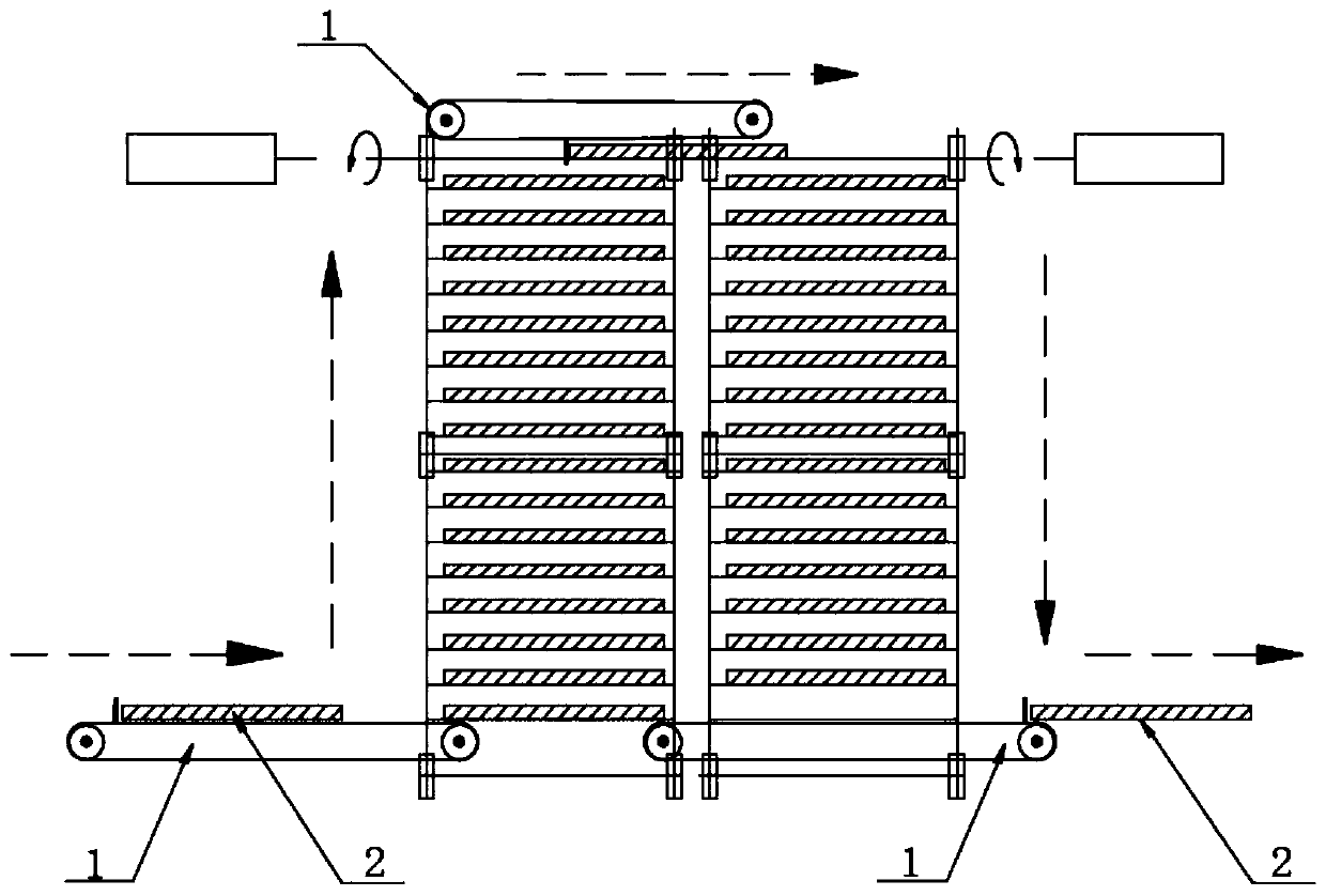
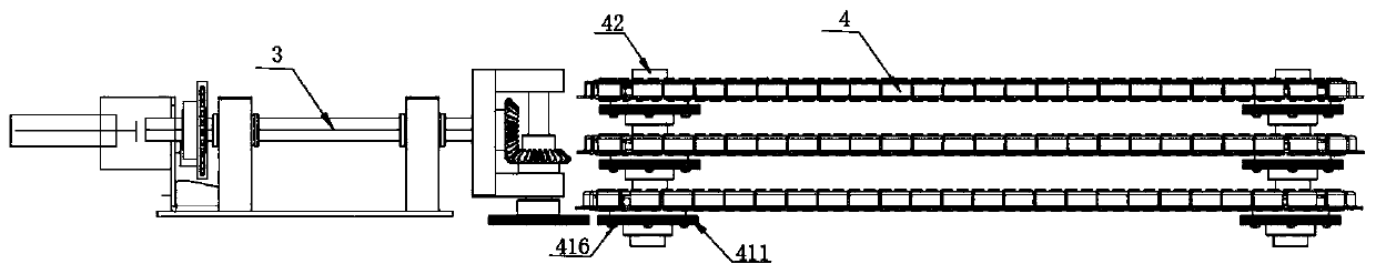
[0026] Such as image 3 , 4 As shown, the PCB transport device of the present invention includes a material rack (not shown in the figure) and a driving mechanism 3 . At least one layer of conveying mechanism 4 is provided on the rack, and each conveying mechanism 4 includes two sets of conveying components 41 for supporting the PCB board 2 and driving the PCB board 2 to move. The two sets of transmission assemblies 41 are arranged in parallel and at intervals, and are all rotatably arranged on the rack, and the two sets of transmission assemblies 41 are driven to rotate by the driving mechanism 3 . The PCB board 2 is supported by two sets of transmission components 41, and the PCB board 2 is driven to move by static friction, so as to avoid the relative sliding between the PCB board 2 and the transmission component 41, so as to avoid th...
PUM
 Abstract
Description
Claims
Application Information
 - R&D
- Intellectual Property
- Life Sciences
- Materials
- Tech Scout
- Unparalleled Data Quality
- Higher Quality Content
- 60% Fewer Hallucinations
Browse by: Latest US Patents, China's latest patents, Technical Efficacy Thesaurus, Application Domain, Technology Topic, Popular Technical Reports.
© 2025 PatSnap. All rights reserved.Legal|Privacy policy|Modern Slavery Act Transparency Statement|Sitemap|About US| Contact US: help@patsnap.com