

OLED display screen, display panel, and manufacturing method thereof
A technology for display panels and array substrates, applied in semiconductor/solid-state device manufacturing, electrical components, electrical solid-state devices, etc., can solve the problems of high production cost, low production efficiency, and long time consumption, so as to improve production efficiency and reduce production costs. , the effect of shortening the process manufacturing time
- Summary
- Abstract
- Description
- Claims
- Application Information
AI Technical Summary
Problems solved by technology
Method used
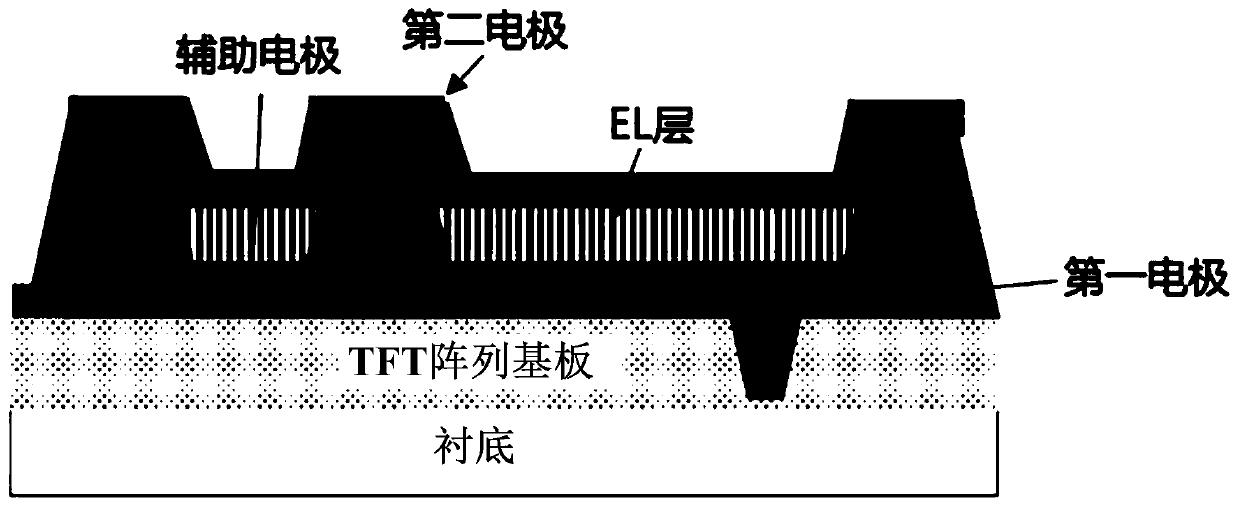
Image

Examples
Embodiment Construction
[0030] In order to make the object, technical solution and advantages of the present invention clearer, the present invention will be described in further detail below in conjunction with specific embodiments and with reference to the accompanying drawings.
[0031] Embodiments of the present invention are described in detail below, examples of which are shown in the drawings, wherein the same or similar reference numerals designate the same or similar elements or elements having the same or similar functions throughout. The embodiments described below by referring to the figures are exemplary only for explaining the present invention and should not be construed as limiting the present invention.
[0032] Those skilled in the art will understand that unless otherwise stated, the singular forms "a", "an", "said" and "the" used herein may also include plural forms. The expression "and / or" used herein includes all or any element and all combinations of one or more associated list...
PUM
 Abstract
Description
Claims
Application Information