Method and system for adding reverse exposure assist feature

A technology of auxiliary graphics and reverse exposure, which is applied in the photo-engraving process of optics, pattern surface, and originals for opto-mechanical processing. window and other issues, to reduce risks and improve the effect of process window

Active Publication Date: 2019-11-19
SHANGHAI HUALI INTEGRATED CIRCUTE MFG CO LTD
View PDF4 Cites 2 Cited by
  • Summary
  • Abstract
  • Description
  • Claims
  • Application Information

AI Technical Summary

Problems solved by technology

However, since the risk of SRAF being exposed to silicon wafers in different environments is different, adding the same parameter SRAF is not an optimal result for the main pattern in different environments, so the process window of the main pattern in each environment cannot be maximized.
In addition, when it is allowed to add a reverse exposure auxiliary pattern on the layout, it is added to the center of the layout based on rules, but the center position is not necessarily the best position for SRAF, which may result in the same size of SRAF on the silicon wafer. It was exposed on the Internet, and finally when selecting the SRAF size, it will be selected in the direction of a small size, which will weaken the effect of SRAF on the main graphics, and it is very limited to improve the process window

Method used


Image

  • Method and system for adding reverse exposure assist feature
  • Method and system for adding reverse exposure assist feature
  • Method and system for adding reverse exposure assist feature

Examples


no. 1 example

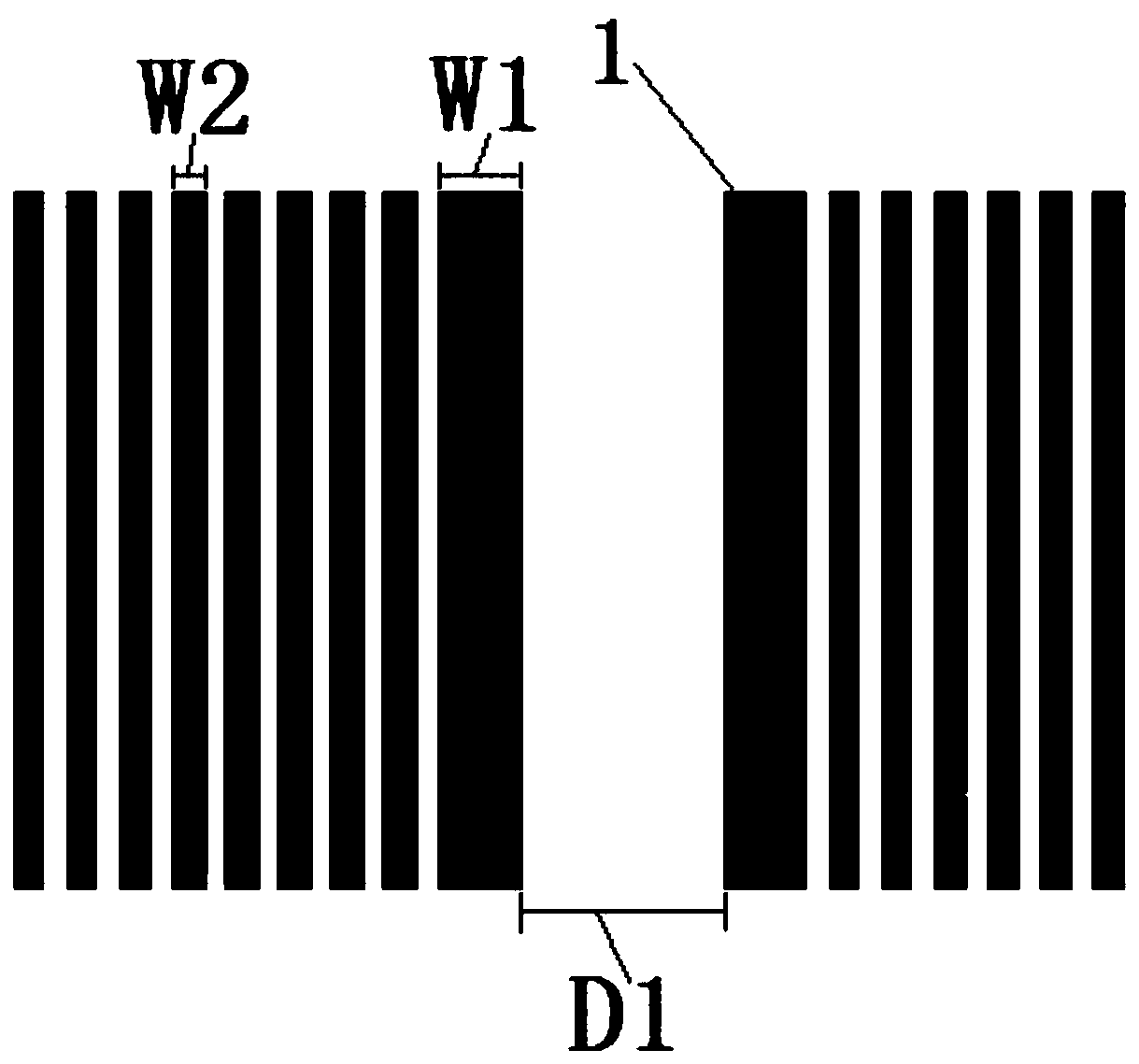
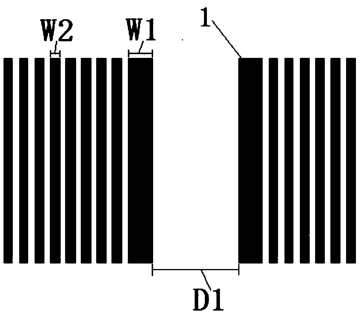
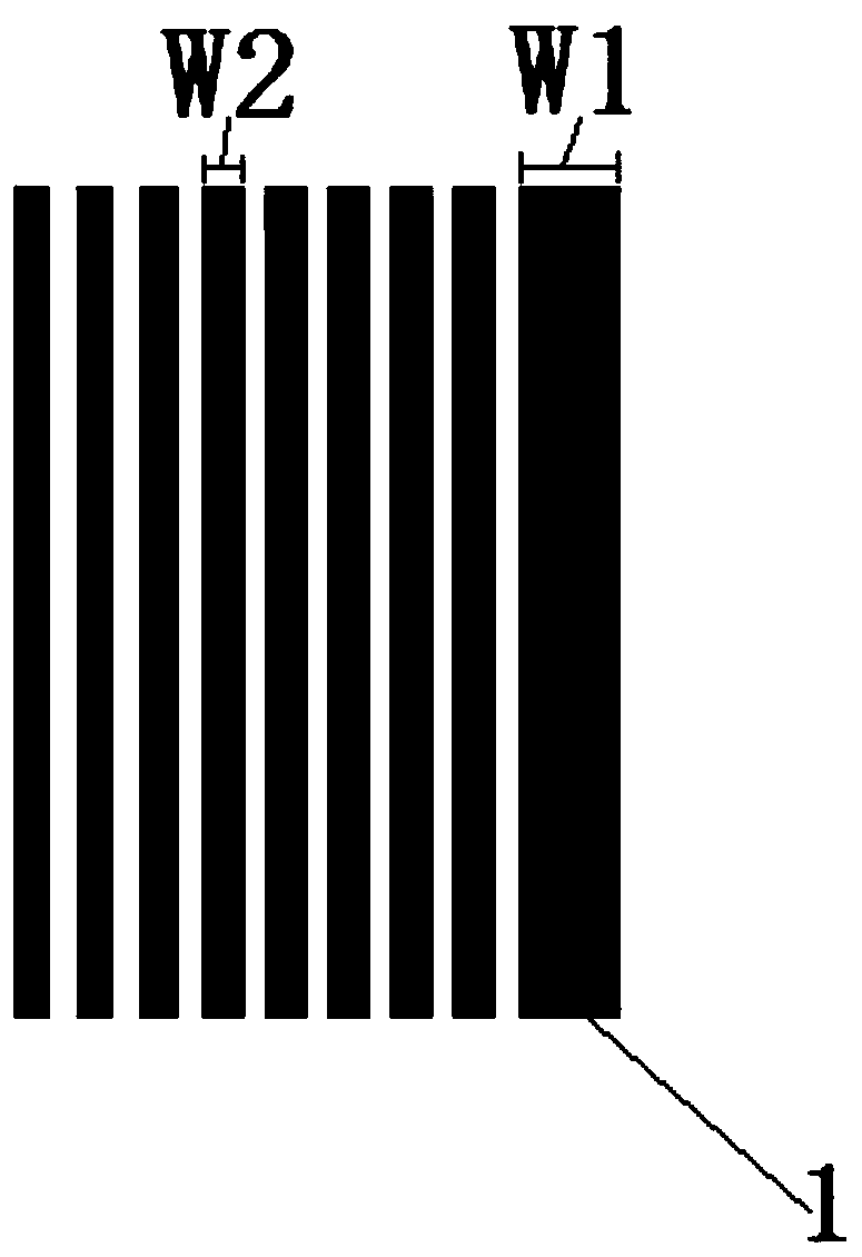
[0044] The present invention provides the first embodiment of the method for adding reverse exposure auxiliary graphics for the linear test layout of semiconductor chips, including the following steps:

[0045] S1, filter out the area where the reverse exposure auxiliary graphics are added at the edge of the test layout through logical operations;

[0046] S2, according to the distance between the edge lines of the test layout, the reverse exposure auxiliary graphic addition area is divided into different reverse exposure auxiliary graphic addition types;

[0047] S3, determining the parameter range for adding reverse exposure auxiliary graphics according to the established process window OPC model;

[0048] S4, obtaining the process fluctuation bandwidth value (PV-band) obtained after adding reverse exposure auxiliary graphics based on the process window OPC model as the process window size evaluation standard;

[0049] S5, add reverse exposure auxiliary graphics of differen...

no. 2 example

[0051] The present invention provides the second embodiment of the reverse exposure auxiliary pattern adding method for the linear test layout of the semiconductor chip, comprising the following steps:

[0052] S1, screen out the area with the line width of the edge line greater than or equal to N times the line width of its adjacent lines on the edge of the test layout through logical operation as the area to add the reverse exposure auxiliary graphics, N>1.

[0053] S2, according to the distance between the edge lines of the test layout, the reverse exposure auxiliary graphic addition area is divided into different reverse exposure auxiliary graphic addition types;

[0054] S3, determining the parameter range for adding reverse exposure auxiliary graphics according to the established process window OPC model;

[0055] S4, obtaining the process fluctuation bandwidth value (PV-band) obtained after adding reverse exposure auxiliary graphics based on the process window OPC model...

no. 3 example

[0057] The present invention provides the third embodiment of the reverse exposure auxiliary pattern adding method for the linear test layout of the semiconductor chip, comprising the following steps:

[0058] S1, screen the edge of the test layout through logical operations, and select the area where the line width of the edge line is greater than or equal to 2.5 times the line width of its adjacent line as the area to add the reverse exposure auxiliary graphics.

[0059] S2, according to the distance between the edge lines of the test layout, the addition type is divided in the following way;

[0060] D1≤(A×W1), then the addition area of ​​the reverse exposure auxiliary figure is divided into the first type of addition type;

[0061] (A×W1)

[0062] (B×W1)≤D1, then the addition area of ​​the reverse exposure auxiliary figure is divided into the thir...


PUM


Abstract

The invention discloses a method for adding a reverse exposure assist feature to a semiconductor chip linear test layout, which comprises: screening out a reverse exposure assist feature addition area; classifying the reverse exposure assist feature addition area into different reverse exposure assist feature addition types based on a distance between the edge lines of the test layout; determininga parameter range of adding the reverse exposure assist feature according to an established process window OPC model; acquiring a PV-band value obtained by adding the reverse exposure assist featurebased on the OPC model as a process window size evaluation standard; adding different sizes of reverse exposure assist features to different reverse exposure assist feature addition types, in order that the layout obtained by adding the reverse exposure assist features based on a design rule conforms to the process window size evaluation standard. The method can improve the process window of the main features in various line width environments, and can avoid the defect that the addition of same parameter SRAF causes the main features in different line width environments to be unable to producethe optimal assist feature.

Description

technical field [0001] The present invention relates to the field of semiconductor manufacturing, in particular to a method for improving the resolution of a photolithography process by adding a sub-resolution exposure assistance pattern (SRAF: Sub-resolution-assist-feature) to a linear test layout of a semiconductor chip. Add method to exposure assist graph. The invention also relates to a reverse exposure auxiliary pattern addition system for improving the resolution of the photolithography process by adding sub-resolution exposure auxiliary patterns to the linear test layout of the semiconductor chip. Background technique [0002] With the continuous reduction of semiconductor manufacturing process technology nodes, sub-resolution exposure assist features (SRAF: Sub-resolution-assist-feature) are usually added to improve the resolution of the lithography process, and the depth of field (DOF, depth of focus) of the graphics , semi-dense (semi-dense) and isolated (iso) gra...

Claims


Application Information

Patent Timeline
Patent Type & Authority Applications(China)
IPC IPC(8): G03F1/36
CPCG03F1/36
Inventor 邹先梅于世瑞
Owner SHANGHAI HUALI INTEGRATED CIRCUTE MFG CO LTD
Why Eureka
Try Eureka