Substrate, preparation method thereof and display device

A substrate and substrate technology, applied in optics, instrumentation, electrical digital data processing, etc., can solve problems such as complex substrate structure, complex preparation process, and restrictions on substrate light and thin design, and achieve the effect of simplifying the structure

Pending Publication Date: 2019-11-19
BOE TECH GRP CO LTD +1
View PDF4 Cites 4 Cited by
  • Summary
  • Abstract
  • Description
  • Claims
  • Application Information

AI Technical Summary

Problems solved by technology

[0003] However, the structure of the current substrate with a touch control structure is relatively complicated, which limits the thinner and thinner design of the substrate, and the manufacturing process is complicated. In addition, the distance between the touch structure and the touch object (such as a finger) is relatively large, and the touch function is limited. low sensitivity

Method used


Image

  • Substrate, preparation method thereof and display device
  • Substrate, preparation method thereof and display device
  • Substrate, preparation method thereof and display device

Examples


preparation example Construction

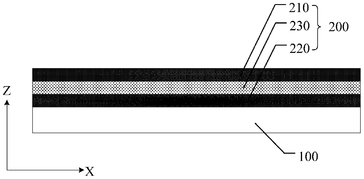
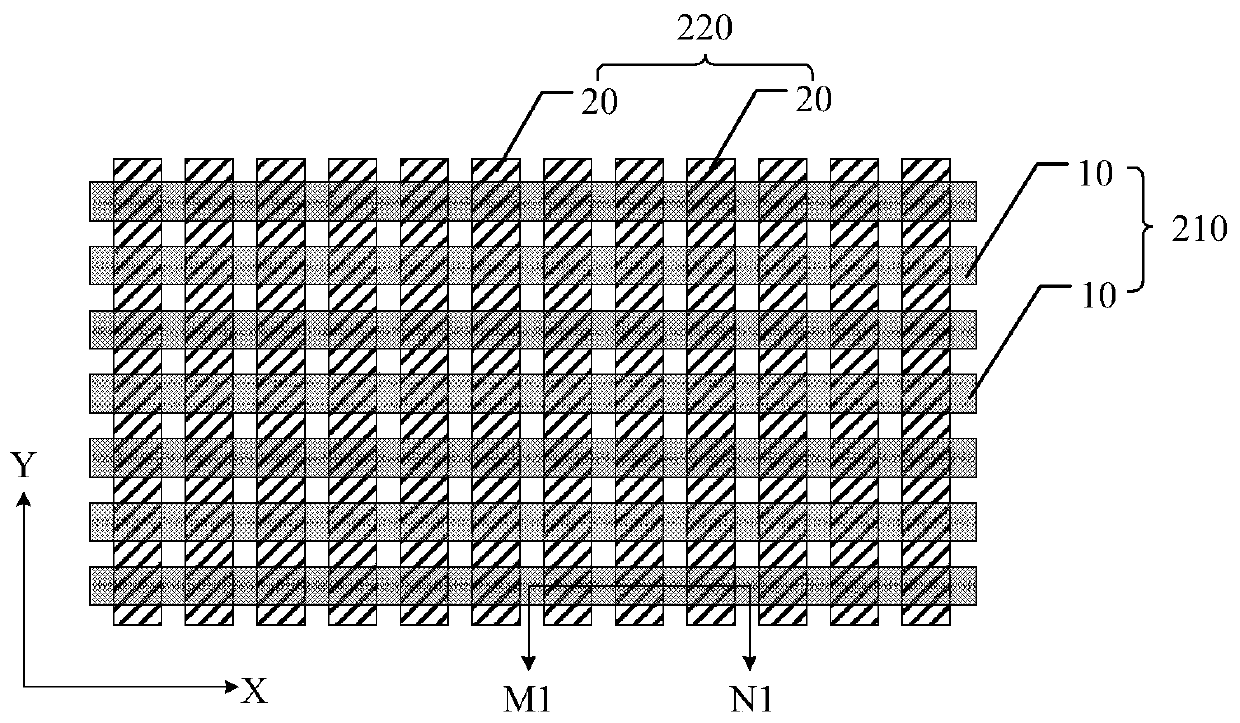
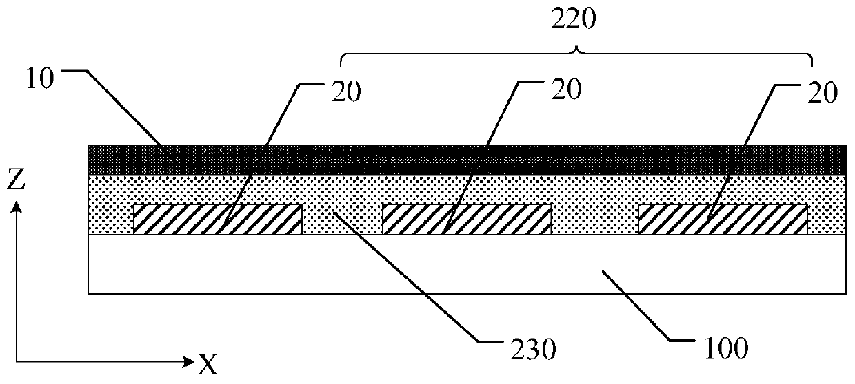
[0080] At least one embodiment of the present disclosure provides a method for preparing a substrate, including: providing a base; and forming a touch structure layer, including: forming the touch structure layer on the base, the touch structure layer including a first electrode layer 1. A laminate of a color filter layer and a second electrode layer; wherein the color filter layer is formed between the first electrode layer and the second electrode layer. For example, a color filter layer is formed as an insulating layer. In the substrate obtained by the above preparation method, the color filter layer is formed in the touch structure layer, and serves as an insulating layer between the first electrode layer, the color filter layer, and the second electrode layer, so that there is no need for the touch structure layer In addition, forming an additional color filter layer can simplify the structure of the substrate, simplify the manufacturing process of the substrate, facilita...


PUM


Abstract

The invention relates to a substrate, a preparation method thereof and a display device, the substrate comprises a base and a touch control structure layer located on the base, the touch control structure layer comprises a first electrode layer, a color filter layer and a second electrode layer which are stacked on the base; wherein the color filter layer is located between the first electrode layer and the second electrode layer, and the color filter layer is integrated in the touch structure layer, so that the structure of the substrate can be simplified, and the light and thin design of thesubstrate is facilitated.

Description

technical field [0001] At least one embodiment of the present disclosure relates to a substrate, a manufacturing method thereof, and a display device. Background technique [0002] Electronic display products with touch functions are increasingly favored by consumers. At present, the more common technologies include resistive, capacitive and optical. Among them, the capacitive touch panel has high accuracy, multi-touch, Features such as high durability and high touch resolution have become the mainstream touch technology used in mid-to-high-end consumer electronics products. [0003] However, the structure of the current substrate with a touch control structure is relatively complicated, which limits the thinner and thinner design of the substrate, and the manufacturing process is complicated. In addition, the distance between the touch structure and the touch object (such as a finger) is relatively large, and the touch function is limited. The sensitivity is low. Content...

Claims


Application Information

Patent Timeline
Patent Type & Authority Applications(China)
IPC IPC(8): G06F3/041G06F3/044
CPCG06F3/041G06F3/044G06F2203/04103G06F2203/04111G06F3/0443G06F3/0446G06F3/0412G06F2203/04112G02F1/13338G02F1/133514H10K59/38H10K59/40G06F3/0448G02F1/133512H10K71/00
Inventor 戴明李易峰刘红灿曹鑫陈竹樊浩原尹正民
Owner BOE TECH GRP CO LTD
Why Eureka
Try Eureka