Display substrate, manufacturing method thereof and display device

A technology of a display substrate and a manufacturing method, which is applied in the directions of semiconductor devices, electrical components, circuits, etc., can solve the problems such as the excessive size of the display panel frame.

Active Publication Date: 2019-11-22
BOE TECH GRP CO LTD
View PDF4 Cites 2 Cited by
  • Summary
  • Abstract
  • Description
  • Claims
  • Application Information

AI Technical Summary

Problems solved by technology

[0003] The present invention at least partly solves the problem that the frame size of the existing OLED display panel is too large, and provides a display substrate, a display device, and a method for manufacturing a display substrate

Method used


Image

  • Display substrate, manufacturing method thereof and display device
  • Display substrate, manufacturing method thereof and display device
  • Display substrate, manufacturing method thereof and display device

Examples


Embodiment 1

[0028] refer to Figure 1f with Figure 2d , this embodiment provides a display substrate, including a base 1 and a plurality of light emitting elements arranged on the base 1, each light emitting element participates in forming a pixel (for black and white display) or a sub-pixel (for color display) ).

[0029] The display substrate has a display surface and multiple side surfaces connected to the display surface. by Figure 1f Taking the current viewing angle as an example, the upper surface of the display substrate is the light emitting surface (for the case of top emission), and the left surface of the display substrate is a side surface.

[0030] The display substrate is divided into a central display area P2 and a plurality of edge display areas P1 located outside the central display area P2, and each edge display area P1 corresponds to a side surface. If the overall shape of the light emitting surface of the display substrate is rectangular, it has four sides, and e...

Embodiment 2

[0039] This embodiment provides a display device including the display substrate according to Embodiment 1.

[0040] Specifically, the display device can be any product or component with a display function such as an organic light emitting diode (OLED) display panel, a mobile phone, a tablet computer, a television set, a monitor, a notebook computer, a digital photo frame, a navigator, and the like.

[0041] The frame size of at least one side of the display device can be shortened.

Embodiment 3

[0043] see image 3 and combine Figure 1a-Figure 1f as well as Figure 2a-Figure 2d , this embodiment provides a method for manufacturing a display substrate. The display substrate of Example 1 can be manufactured by applying this manufacturing method. The display substrate has a display surface and multiple sides connected to the display surface. The display substrate is divided into a central display area P2 and a plurality of edge display areas P1 located outside the central display area P2. Each edge display area P1 corresponds to a side surface. The manufacturing method includes the following steps.

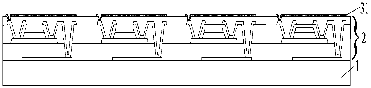
[0044] Step S1 , providing a substrate 1 on which a driving circuit layer 2 is formed, and a plurality of pixel electrodes 31 are exposed on the surface of the driving circuit layer 2 facing away from the substrate 1 .

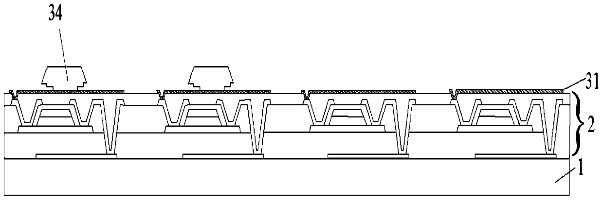
[0045]Step S2, transfer the micro light emitting diode 34 to the pixel electrode 31 in at least one edge display area P1.

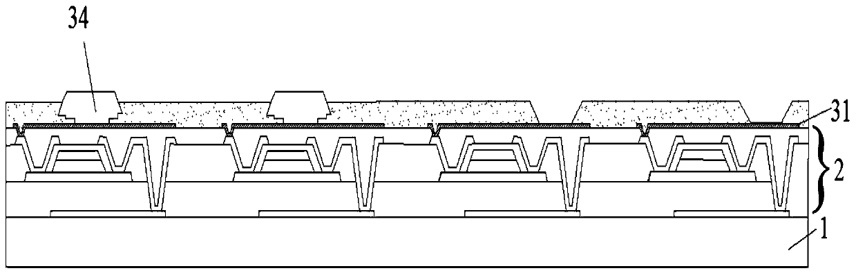
[0046] Step S3 , forming or...


PUM


Abstract

The invention provides a display substrate, a manufacturing method thereof and a display device, and belongs to the technical field of display, at least partially solving the problem that the frame size of an existing organic light emitting diode display panel is difficult to continuously shorten. The display substrate comprises a substrate body and a plurality of light-emitting elements arrangedon the substrate body. Each light-emitting element participates in forming a pixel or a sub-pixel; wherein the display substrate is provided with a display surface and a plurality of side surfaces connected with the display surface; the display substrate is divided into a middle display area and a plurality of edge display areas located on the outer side of the middle display area, each edge display area corresponds to one side face, the light-emitting elements in the middle display area are organic light-emitting diodes, and the light-emitting elements in at least one edge display area are micro light-emitting diodes.

Description

technical field [0001] The invention belongs to the field of display technology, and in particular relates to a display substrate, a display device, and a manufacturing method of a display substrate. Background technique [0002] In an organic light emitting diode (OLED) display panel, since the organic functional layer is sensitive to water and oxygen, it is necessary to cover an encapsulation layer on the organic light emitting diode structure. As a result, the size of the frame of the organic light emitting diode display panel is relatively large, and it is difficult to achieve a narrow frame design. Contents of the invention [0003] The present invention at least partly solves the problem that the frame size of the existing organic light emitting diode display panel is too large, and provides a display substrate, a display device, and a manufacturing method of the display substrate. [0004] According to the first aspect of the present invention, a display substrate ...

Claims


Application Information

Patent Timeline
Patent Type & Authority Applications(China)
IPC IPC(8): H01L27/32
CPCH10K59/00H10K59/123H10K59/12H10K59/1201H01L25/167H10K59/121H10K50/84H10K59/122H10K71/00
Inventor 谢蒂旎
Owner BOE TECH GRP CO LTD
Why Eureka
Try Eureka