Electron beam device and manufacturing method thereof

A manufacturing method and electron beam technology, applied in the field of electronics, can solve the problems of large size and high power consumption, etc.

Pending Publication Date: 2019-06-14
西安众力为半导体科技有限公司
View PDF0 Cites 0 Cited by
  • Summary
  • Abstract
  • Description
  • Claims
  • Application Information

AI Technical Summary

Problems solved by technology

[0004] From the perspective of electrical characteristics, the modulation characteristics, linearity and other indicators of tradition

Method used


Image

  • Electron beam device and manufacturing method thereof
  • Electron beam device and manufacturing method thereof
  • Electron beam device and manufacturing method thereof

Examples


example 1

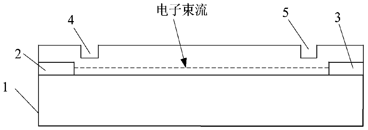
[0035] An insulating layer is provided on the surface of the GaN / AlGaN composite layer, and the modulation input end and the modulation output end include: a window opened on the insulating layer with a preset distance from the cathode and the anode respectively, and depositing A metal layer, wherein the metal layer forms a metal-semiconductor contact with the GaN / AlGaN composite layer.

[0036] Wherein, the insulating layer includes but not limited to Si 3 N 4 In the insulating layer, the width of the window is 0.5-50 microns, and the preset distance is 1-50 microns. For example, when fabricating the modulation input end and the modulation output end according to this embodiment, Si 3 N 4 Si is etched away on the insulating layer 3 N 4 , forming a 0.5 micron wide window, and depositing a metal layer in the window, so that the metal layer forms a metal-semiconductor contact with the GaN / AlGaN composite layer, so as to obtain a modulation input terminal and a modulation ou...

example 2

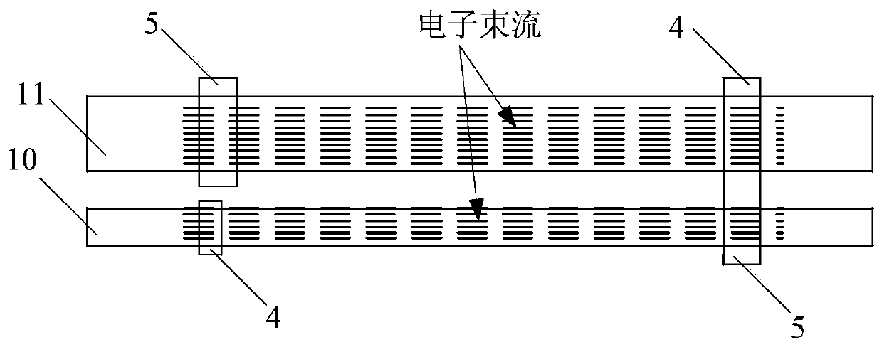
[0038] The surface of the GaN / AlGaN composite layer is provided with an insulating layer, and the modulation input end and the modulation output end include: a window opened on the insulating layer with a preset distance from the cathode and the anode respectively, and a gate deposited in the window A dielectric layer and a metal layer deposited on the gate dielectric layer, wherein the bottom of the window extends into the GaN / AlGaN composite layer.

[0039] Wherein, the insulating layer includes but not limited to Si 3 N 4 insulating layer, the gate dielectric layer may include SiO 2 layer, the SiO 2 The thickness of the layer is 1-500 nanometers, and the preset distance is 1-50 micrometers. For example, when fabricating the modulation input terminal and the modulation output terminal according to this embodiment, Si can be etched away at a distance of 20 microns from the cathode and the anode, respectively. 3 N 4 , and then continue to etch down into the GaN / AlGaN comp...


PUM

PropertyMeasurementUnit
Thicknessaaaaaaaaaa
Thicknessaaaaaaaaaa
Thicknessaaaaaaaaaa

Abstract

The invention relates to an electron beam device and a manufacturing method thereof. The electron beam device comprises a semiconductor substrate and a GaN/AlGaN composite layer on the surface of thesemiconductor substrate, wherein a cathode is arranged at one end of the GaN/AlGaN composite layer, and an anode is arranged at the other end of the GaN/AlGaN composite layer; and a modulation input end and a modulation output end are arranged between the cathode and the anode. Due to the fact that the GaN/AlGaN composite layer is made of a semiconductor material composed of crystal lattice atomswhich are arranged orderly, when voltage bias is applied between the anode and the cathode, the electron beams generated at the heterojunction interface of the GaN/AlGaN composite layer pass through the lattice atoms, and the drift speed is greatly limited, therefore, the operation distance of the electron beams in a period of time is correspondingly reduced, so that the size of the electron beamdevice can be greatly reduced, the miniaturization of the electron beam device is realized, and the problem that the size of a traditional electron beam device is too large is solved.

Description

technical field [0001] The present disclosure relates to the field of electronic technology, in particular, to an electron beam device and a manufacturing method thereof. Background technique [0002] Early electronic technology relied on electron tubes, which consisted of an electron gun and a number of control electrodes, all of which were encapsulated in a vacuum glass tube. When working, a specific voltage bias is applied at both ends of the electron tube, so that the cathode of the electron tube emits an electron beam, and under the traction of the nearby accelerator voltage, an electron beam (also known as an electron beam) is formed. The electron beam flows in a vacuum travels, eventually reaching the anode of the tube and forming a current in the outer circuit loop. [0003] Taking the klystron tube as an example, the above-mentioned electron beam can be modulated by receiving a microwave signal coupled in through the slit near the cathode during its traveling dista...

Claims


Application Information

Patent Timeline
IPC IPC(8): H01J23/09H01J25/10
Inventor 罗景涛严可为
Owner 西安众力为半导体科技有限公司
Why Eureka
Try Eureka