A method for quickly estimating the copper thickness of pcb via holes

A technology for PCB board and surface copper thickness, which is applied to printed circuits, instruments, measuring devices, etc. It can solve the problems of limited test probe size, inability to test copper thickness in holes, and inability to test copper thickness in via holes, etc., to ensure production Quality, the effect of controlling production costs

Active Publication Date: 2022-01-25
福州瑞华印制线路板有限公司
View PDF4 Cites 0 Cited by
  • Summary
  • Abstract
  • Description
  • Claims
  • Application Information

AI Technical Summary

Problems solved by technology

[0004] 1. Hole copper tester: It is a non-destructive test and can be tested quickly. The disadvantage is that the size of the test probe is limited, and it can only test the copper thickness in the hole after electroplating of the component hole with a hole diameter larger than 0.8mm, and the copper thickness tested It is the average value in the component hole instead of the minimum copper thickness value in the center, and it is impossible to test the copper thickness of the via hole with a

Method used


Image

  • A method for quickly estimating the copper thickness of pcb via holes
  • A method for quickly estimating the copper thickness of pcb via holes
  • A method for quickly estimating the copper thickness of pcb via holes

Examples


Embodiment Construction

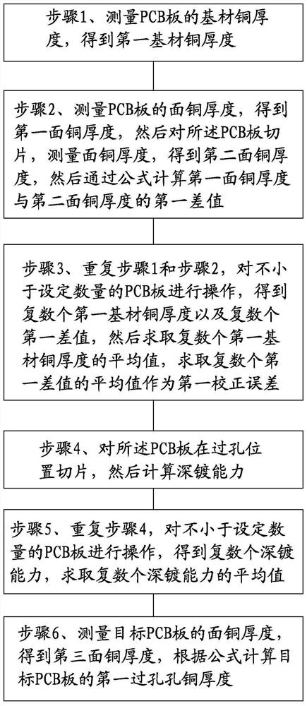
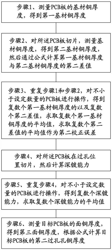
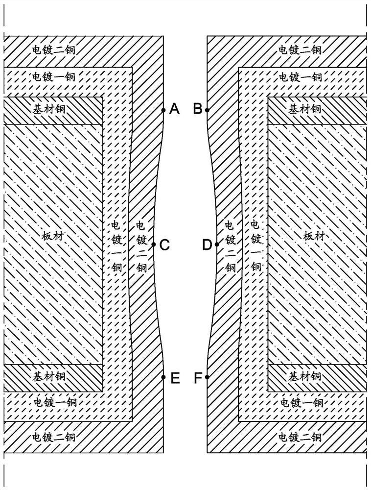
[0052] Please refer to figure 1 , image 3 and Figure 4 , one of the embodiments of the present invention, a method for quickly estimating the copper thickness of a PCB via hole, comprising the following steps:

[0053] A method for rapidly estimating the copper thickness of PCB via holes, comprising the following steps:

[0054] Step 1. Measure the substrate copper thickness of the PCB board at a copper surface position not less than a set area (such as 10mm×10mm) by a surface copper tester to obtain the first substrate copper thickness;

[0055] Step 2. Measure the surface copper thickness of the PCB board at a copper surface position not smaller than the set area (such as 10mm×10mm) by a surface copper tester to obtain the first surface copper thickness, and then use the slicing technology to measure the surface copper thickness of the PCB board on the same surface. Slice the position of the copper surface, measure the copper thickness of the surface, and obtain the cop...


PUM


Abstract

The invention provides a method for quickly calculating the copper thickness of a PCB via hole, comprising: measuring the copper thickness of the surface copper through a surface copper tester, measuring the copper thickness of the via hole through a slicing technique and calculating the deep plating capacity, and the statistics are not less than the designed A certain number of PCB boards are measured, and the average value of surface copper thickness and deep plating ability are obtained respectively, and then the surface copper thickness of the PCB board to be tested is measured by the surface copper tester, and the correction error is also introduced. The measurement results are corrected, and finally the calculation formula can be used to quickly calculate the copper thickness of the via hole center of the PCB board to be tested by measuring the surface copper thickness of the target PCB board. In the case that the PCB board has only via holes, the invention quickly calculates the hole copper thickness in the center of the via hole without destroying the PCB board to be tested.

Description

technical field [0001] The invention relates to a method for testing the electroplating copper thickness of a printed circuit board, in particular to a method for rapidly calculating the copper thickness of PCB via holes. Background technique [0002] Since the 1960s, the printed circuit board (PCB) industry has adopted hole metallization and electroplating technology to solve the problem of interlayer connection or conduction. The via holes and component holes on the PCB need to be electroplated to meet customer requirements. Only the thickness can meet the quality requirements, and copper is the main component that determines the cost of PCB, so how to scientifically control the copper thickness is very important. [0003] The existing copper thickness test methods are as follows: [0004] 1. Hole copper tester: It is a non-destructive test and can be tested quickly. The disadvantage is that the size of the test probe is limited, and it can only test the copper thickness ...

Claims


Application Information

Patent Timeline
IPC IPC(8): H05K3/00G01B21/08
CPCH05K3/00G01B21/08H05K2203/162
Inventor 詹少华陈跃生郭正平张丽芳
Owner 福州瑞华印制线路板有限公司
Why Eureka
Try Eureka