Semiconductor element and manufacturing method thereof

A semiconductor and component technology, applied in the field of making dynamic random access memory components

Active Publication Date: 2019-12-17
UNITED MICROELECTRONICS CORP +1
View PDF6 Cites 2 Cited by
  • Summary
  • Abstract
  • Description
  • Claims
  • Application Information

AI Technical Summary

Problems solved by technology

However, limited by the manufacturing process technology, there are still many defects in the existing DRAM cells with recessed gate structures, which need to be further improved to effectively improve the performance and reliability of related memory components

Method used


Image

  • Semiconductor element and manufacturing method thereof
  • Semiconductor element and manufacturing method thereof
  • Semiconductor element and manufacturing method thereof

Examples


Embodiment Construction

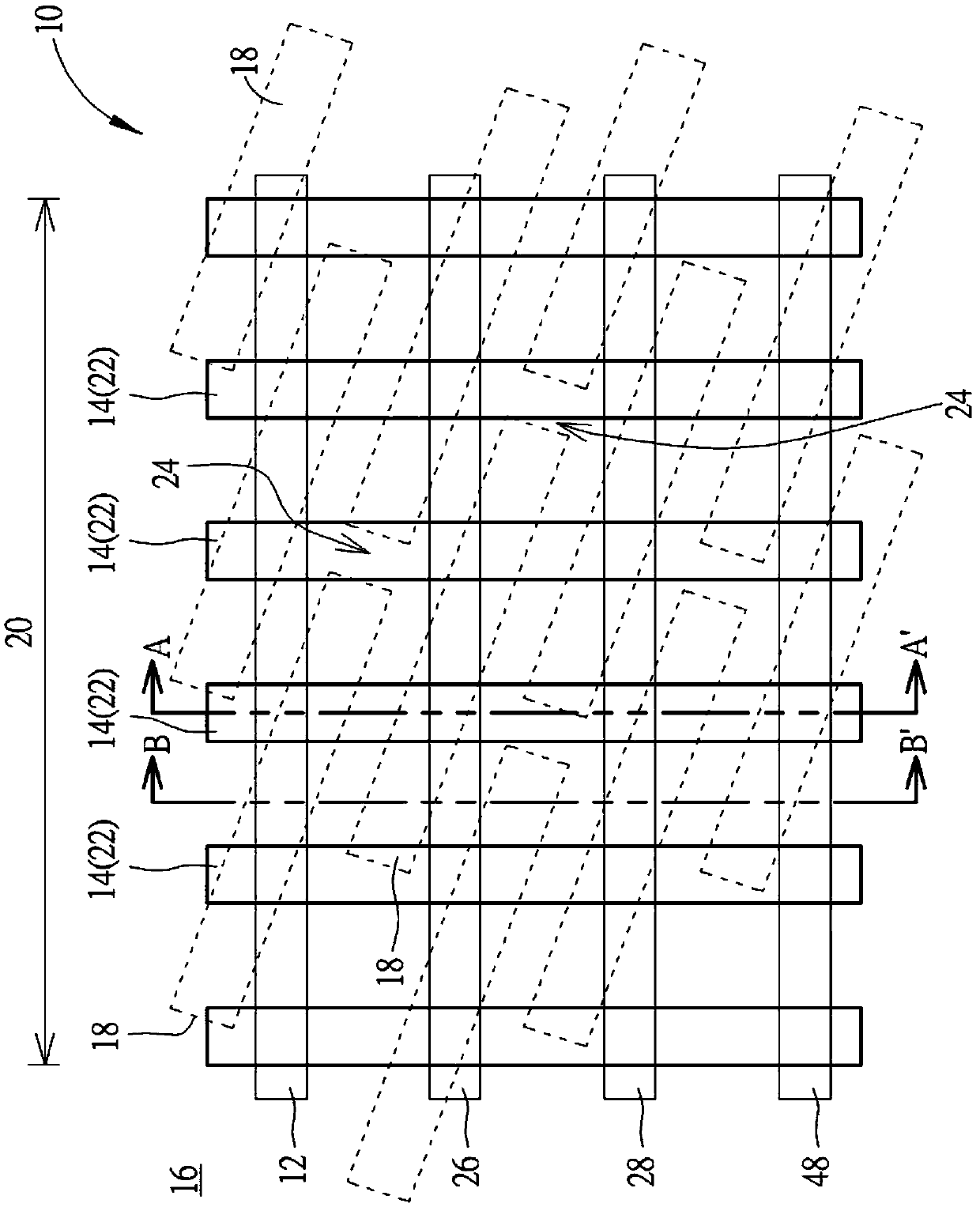
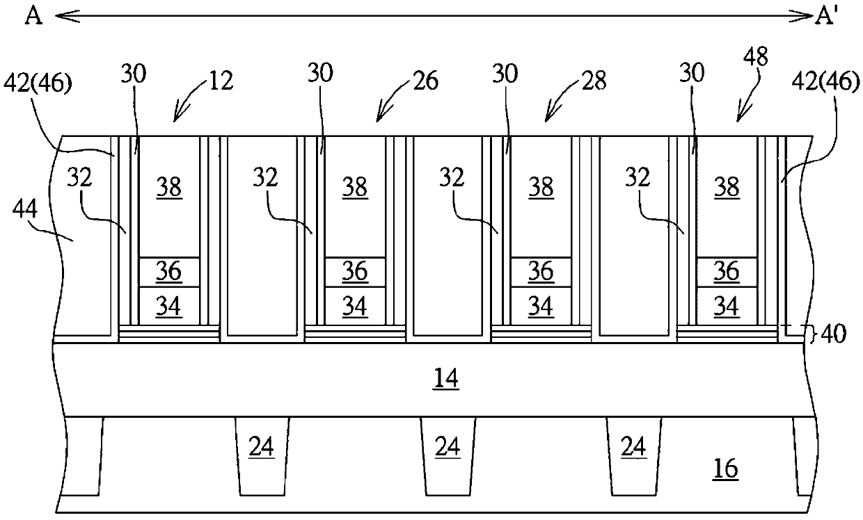
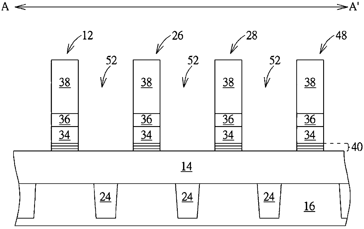
[0027] Please refer to Figure 1 to Figure 8 , Figure 1 to Figure 8 A schematic diagram of a method for making a dynamic random access memory element according to an embodiment of the present invention, wherein figure 1 Make the top diagram of a DRAM dynamic random access memory element for the present invention, Figure 2 to Figure 4 for figure 1 Schematic diagram of the method for fabricating dynamic random access memory elements along the tangent line AA' in , Figure 5 to Figure 7 for figure 1 Schematic diagram of the method for fabricating dynamic random access memory elements along the tangent line BB' in , Figure 8 then figure 1 The enlarged top view of a part located between two adjacent bit line structures in .

[0028] This embodiment provides a memory element, such as a DRAM element 10 with a recessed gate, which includes at least one transistor element (not shown) and at least one capacitor structure (not shown), so as to As the smallest constituent unit i...


PUM


Abstract

The invention discloses a semiconductor element and a manufacturing method thereof. The method for manufacturing the semiconductor element mainly comprises the steps of firstly, forming a first bit line structure on a substrate, forming a first gap wall beside the first bit line structure, forming an interlayer dielectric layer beside the first gap wall, removing part of the interlayer dielectriclayer and part of the first gap wall and exposing the side wall of the first bit line structure, and then forming a first storage node contact isolation structure beside the first bit line structure,wherein the first storage node contact isolation structure is directly contacted with the first bit line structure and the first gap wall.

Description

technical field [0001] The invention relates to a method for manufacturing a semiconductor element, in particular to a method for manufacturing a Dynamic Random Access Memory (Dynamic Random Access Memory, DRAM) element. Background technique [0002] With the trend of miniaturization of various electronic products, the design of dynamic random access memory (DRAM) cells must also meet the requirements of high integration and high density. For a DRAM cell with a recessed gate structure, since it can obtain a longer carrier channel length in the same semiconductor substrate to reduce the leakage of the capacitor structure, it is under the current mainstream development trend , which has gradually replaced DRAM cells with only planar gate structures. [0003] Generally, a DRAM cell with a recessed gate structure includes a transistor element and a charge storage device for receiving voltage signals from bit lines and word lines. However, due to the limitation of manufacturing...

Claims


Application Information

Patent Timeline
Patent Type & Authority Applications(China)
IPC IPC(8): H01L21/8242H01L27/108
CPCH10B12/30H10B12/09H10B12/50H10B12/315H10B12/0335H10B12/482H01L21/762H10B12/485H10B12/488
Inventor 吴柏翰李甫哲蔡建成刘姿岑吕文杰
Owner UNITED MICROELECTRONICS CORP
Why Eureka
Try Eureka