Chip test system and test method

A test system and chip technology, applied in the direction of static memory, instruments, etc., can solve the problems of small number of chip tests, high test costs, and small number of test machines, to achieve efficient parallel test capabilities and solve test costs High, flexible and adjustable effects

Active Publication Date: 2019-12-31
珠海博雅科技股份有限公司
View PDF8 Cites 13 Cited by
  • Summary
  • Abstract
  • Description
  • Claims
  • Application Information

AI Technical Summary

Problems solved by technology

At present, although the test machines on the market usually have full functions and high performance, the number of simultaneous tests of these test machines is small and the price is expensive, so chip testing faces the technica

Method used


Image

  • Chip test system and test method
  • Chip test system and test method
  • Chip test system and test method

Examples


Embodiment Construction

[0038] The present invention is described below based on examples, but the present invention is not limited to these examples. In the following detailed description of the invention, some specific details are set forth in detail. The present invention can be fully understood by those skilled in the art without the description of these detailed parts. In order to avoid obscuring the essence of the present invention, well-known methods, procedures, and flow charts are not described in detail. Additionally, the drawings are not necessarily drawn to scale.

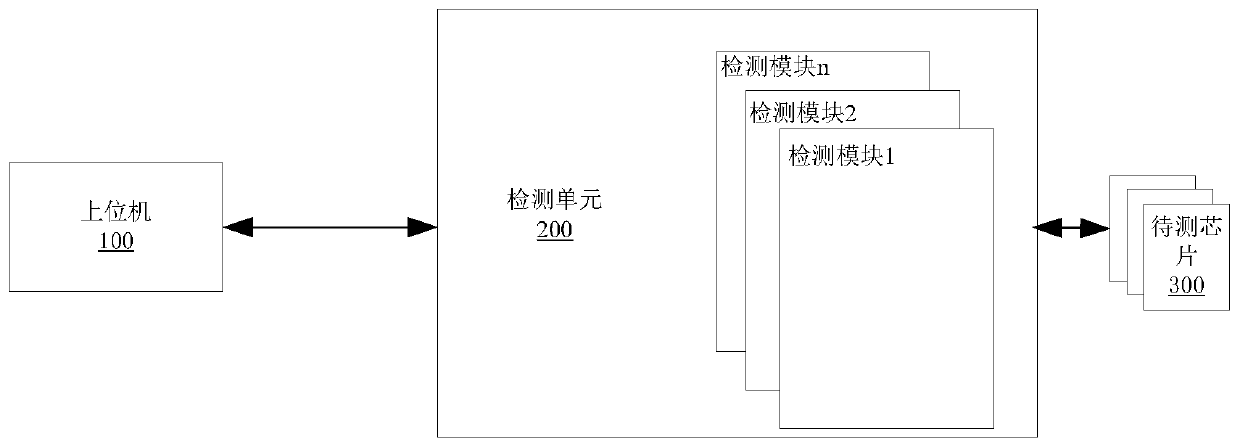
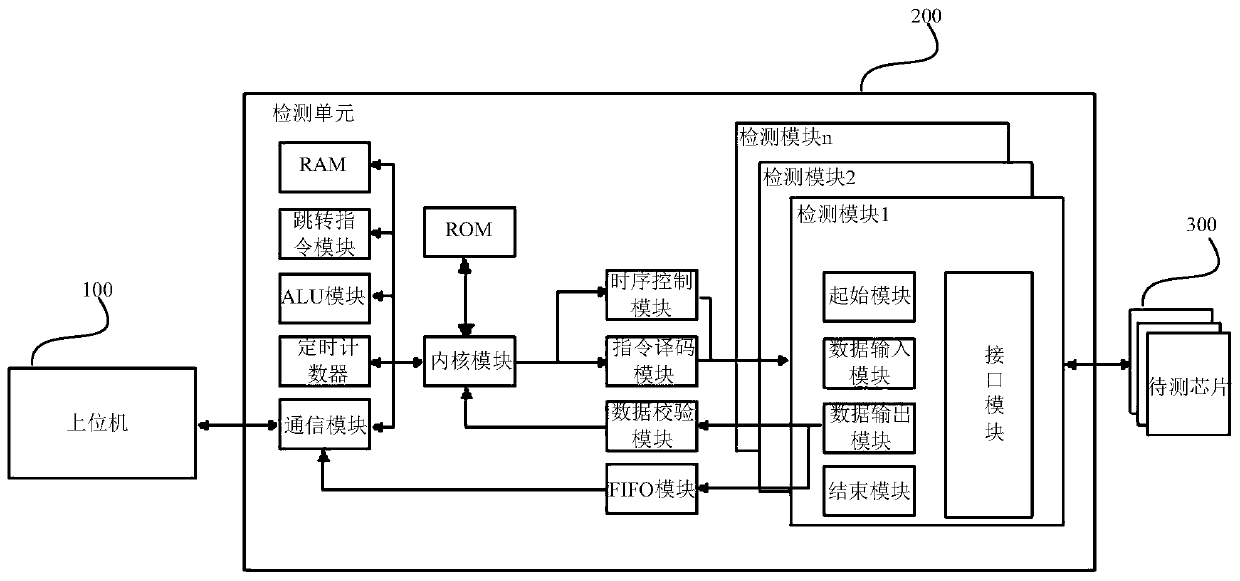
[0039] figure 1 Shown is a chip testing system provided by the embodiment of the present invention. refer to figure 1 , chip test system, including:

[0040] A test unit 200, the test unit 200 is built by an FPGA chip and configured with a plurality of parallel test modules, and the test modules and the chip 300 to be tested are in a one-to-one correspondence;

[0041] The host computer 100 connected with the test unit 2...


PUM


Abstract

The embodiment of the invention provides a chip test system and test method. The test system comprises an upper computer and a test unit which are in communication connection with each other. The testunit is built by an FPGA chip and is configured with a plurality of parallel test modules, and the test modules are in one-to-one correspondence with to-be-tested chips. The test unit writes a test function through an upper computer, and the test function is a function written based on a custom instruction set; wherein the upper computer sends a start instruction to the test unit, the test unit operates the test function after receiving the start instruction so as to call the plurality of test modules to test the corresponding chips to be tested respectively, and test results obtained based on output data of the chips to be tested are sent to the upper computer. The chip test system and the test method provided by the embodiment of the invention are based on an FPGA hardware system and test is carried out through the test function written by the custom instruction set, so that the technical problems of a small number of chips under the same test and high test cost are solved.

Description

technical field [0001] The invention relates to the technical field of semiconductors, in particular to a chip testing system and testing method. Background technique [0002] Chips, also known as microcircuits, microchips, and integrated circuits, generally refer to the carrier of an integrated circuit and are an independent whole that can be used directly. With the improvement of the integration level of electronic products, more and more types of chips are involved in the design of electronic products, such as memory chips, which include volatile memory chips and non-volatile memory chips. [0003] Non-volatile memory chips are widely used as a memory chip that can still retain stored content when the chip is powered off. The non-volatile memory chips are tested before leaving the factory or before use, including functional and reliability tests, and these tests of the non-volatile memory chips generally require a large number of test samples and many test functions. At...

Claims


Application Information

Patent Timeline
IPC IPC(8): G11C29/56
CPCG11C29/56
Inventor 安友伟郭润森闫江李迪陈刚张登军刘大海李建球余作欢逯钊琦
Owner 珠海博雅科技股份有限公司
Why Eureka
Try Eureka