A high voltage p-channel hfet device

A channel and device technology, applied in the field of p-channel HFET devices, can solve the problems of limited breakdown voltage increase and difficult process, and achieve the effects of small on-resistance, parasitic capacitance of the withstand voltage structure, and high breakdown voltage

Active Publication Date: 2021-04-02
UNIV OF ELECTRONICS SCI & TECH OF CHINA
View PDF5 Cites 0 Cited by
  • Summary
  • Abstract
  • Description
  • Claims
  • Application Information

AI Technical Summary

Problems solved by technology

[0004] Aiming at the shortcomings of the withstand voltage structure proposed for HFET devices in the prior art, such as high process difficulty and limited breakdown voltage improvement, the present invention provides a p-channel with a comb finger-shaped n-type surface withstand voltage structure connected to the source HFET device

Method used


Image

  • A high voltage p-channel hfet device
  • A high voltage p-channel hfet device
  • A high voltage p-channel hfet device

Examples


Embodiment

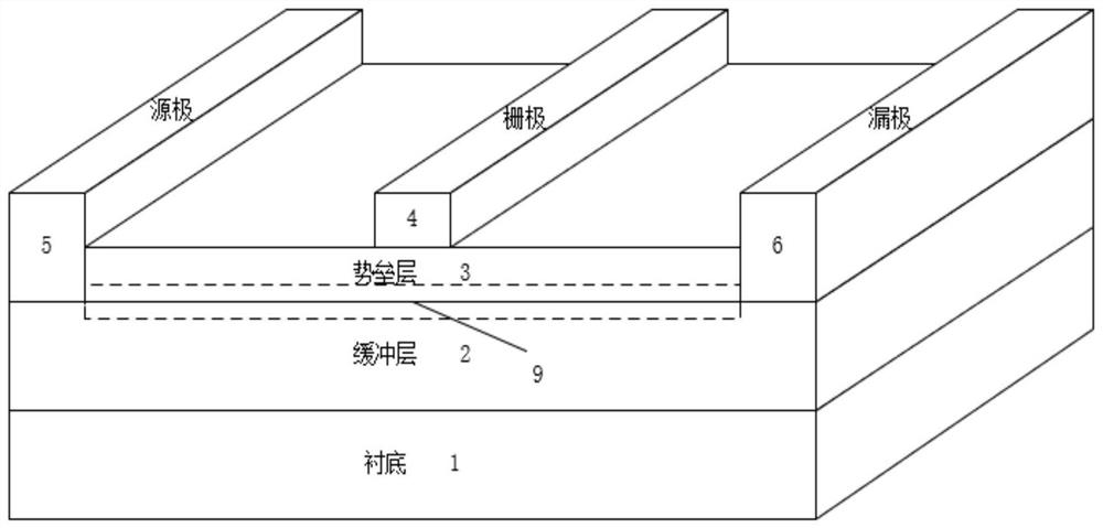
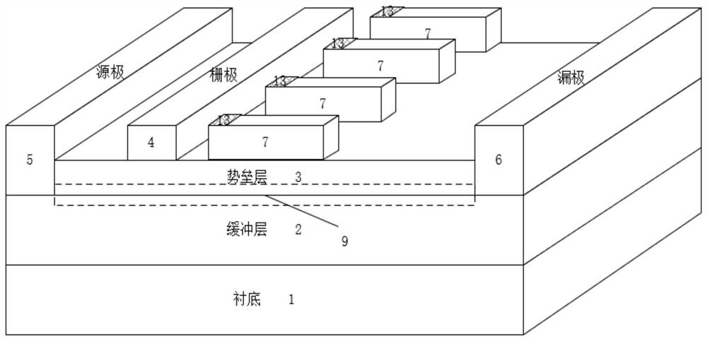
[0043] The present invention provides a p-channel HFET device with a comb finger-shaped n-type surface withstand voltage structure connected to the source, including a substrate 1, a buffer layer 2, a barrier layer 3, a gate 4, a source 5 and a drain electrode 6, a buffer layer 2 and a barrier layer 3 are sequentially arranged on the substrate 1, and a two-dimensional conductive channel 9 is formed at the interface between the barrier layer 3 and the buffer layer 2; the source electrode 5 and the drain electrode 6 are respectively arranged on the HFET device Both sides form an ohmic contact with the two-dimensional conductive channel 9; a gate 4 is arranged between the source 5 and the drain 6, and the gate 4 is located on the barrier layer 3 to form a Schottky contact with the barrier layer 3; The area between the gate 4 and the drain 6 on the barrier layer 3 is provided with a plurality of n-type semiconductor blocks 7 distributed in a finger shape, and each n-type semiconduc...


PUM


Abstract

A high-voltage p-channel HEMT device belongs to the technical field of semiconductor power devices. In view of the relatively high process difficulty in preparing a superjunction on a heterojunction device such as a HEMT, the present invention proposes a surface superjunction structure for a p-channel HEMT device, by preparing a finger-shaped n-type junction on the surface of the drift region of the device. Semiconductor strips, and the n-type semiconductor strips are electrically connected to the source, and the drift region channel can be depleted in a large range under the off condition, and the depletion region can withstand higher voltage, so that the device breaks down Features are enhanced. On the other hand, since the finger-shaped n-type surface withstand voltage structure connected to the source only covers a small area of ​​the drift region, when the device is turned on, the associated parasitic resistance and parasitic capacitance are relatively small, which makes the device have Relatively good DC conduction characteristics and high frequency characteristics.

Description

technical field [0001] The invention belongs to the technical field of semiconductor power devices, in particular to a p-channel HFET device with a comb finger-shaped n-type surface withstand voltage structure connected to a source. Background technique [0002] In the field of radio frequency and power integrated circuits, with the continuous improvement of the integration level of the circuit, the circuit has higher and higher requirements for the characteristics of the device. When the performance of traditional silicon devices has almost reached the theoretical limit, it is urgent to develop a new device with high frequency, high speed, high power, low noise and low power consumption to meet the needs of high-speed and large-capacity computers and large-capacity long-distance To meet the requirements of communication, semiconductor heterojunction devices came into being. Among them, the heterojunction field effect transistor (Heterostructure Field-Effect Transistor, HFE...

Claims


Application Information

Patent Timeline
Patent Type & Authority Patents(China)
IPC IPC(8): H01L29/778H01L29/06
CPCH01L29/0607H01L29/0684H01L29/778
Inventor 罗谦姜玄青文厚东孟思远
Owner UNIV OF ELECTRONICS SCI & TECH OF CHINA
Why Eureka
Try Eureka