Digital pin conversion device and method based on FPGA

A technology of a conversion device and a conversion method, which is applied in the fields of electrical digital data processing, digital computer components, and architecture with a single central processing unit, etc. Effect

Active Publication Date: 2020-01-10
BEIJING SMARTCHIP MICROELECTRONICS TECH COMPANY +2
View PDF5 Cites 1 Cited by
  • Summary
  • Abstract
  • Description
  • Claims
  • Application Information

AI Technical Summary

Problems solved by technology

However, since it is impossible to understand or meet all users' needs for pin layout during chip desig...

Method used


Image

  • Digital pin conversion device and method based on FPGA
  • Digital pin conversion device and method based on FPGA
  • Digital pin conversion device and method based on FPGA

Examples


Embodiment Construction

[0016] The specific embodiments of the present invention will be described in detail below in conjunction with the accompanying drawings, but it should be understood that the protection scope of the present invention is not limited by the specific embodiments.

[0017] Unless expressly stated otherwise, throughout the specification and claims, the term "comprise" or variations thereof such as "includes" or "includes" and the like will be understood to include the stated elements or constituents, and not Other elements or other components are not excluded.

[0018] In order to overcome the problems in the prior art, the present invention provides a digital pin conversion device and method based on FPGA (Field Programmable Logic Gate Array), which can perform arbitrary Conversion can improve the flexibility of chip pins and save chip costs.

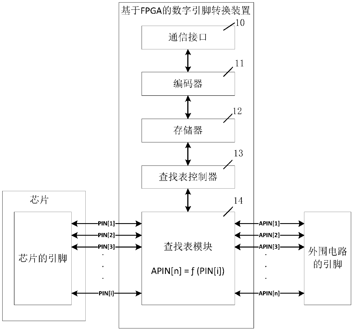
[0019] figure 1 It is an FPGA-based digital pin conversion device according to an embodiment of the present invention.

[0020] The FPG...


PUM


Abstract

The invention discloses a digital pin conversion device and method based on an FPGA. The device comprises a communication interface, an encoder, a memory, a lookup table controller and a lookup tablemodule. The communication interface receives externally input pin configuration data, wherein the pin configuration data comprises pin data of the chip and pin data of a peripheral circuit. The encoder encodes the pin configuration data according to the pin configuration requirement of the peripheral circuit so as to generate a two-dimensional relationship data table in one-to-one correspondence between the encoded chip pins and the pins of the peripheral circuit. The memory stores the two-dimensional relationship data table, and the lookup table controller reads the address information and the data information in the memory so as to control the lookup table module to select the connection relationship between the pin of the chip and the pin of the peripheral circuit. According to the digital pin conversion device and method based on an FPGA, random arrangement of existing pins of the chip can be realized through random configuration of software on the existing pin resources of the chip, and the cost is reduced.

Description

technical field [0001] The invention relates to the field of chip design, in particular to an FPGA-based digital pin conversion device and method. Background technique [0002] With the expansion of the chip scale, the number of chip pins is also increasing, and the function multiplexing on the same pin becomes more and more, sometimes 7-8 functions are multiplexed on one pin, or even more . In the existing technical solution, the pins of the MCU chip are configured through registers, and the chip user selects from several functions given on a certain pin of the MCU chip according to the application requirements. Therefore, the peripheral application circuit design of the chip also becomes more complicated, and it is impossible to achieve the same pin as a certain chip, so the application circuit needs to be redesigned for the replacement of alternative chips. [0003] Based on the existing technical solutions, the pins of the chip products require the chip user to select ...

Claims


Application Information

Patent Timeline
IPC IPC(8): G06F15/78
CPCG06F15/7832
Inventor 黎金旺张彦欣贺龙龙宁振海杨小坤刘硕李德建杨立新谭浪于宝东
Owner BEIJING SMARTCHIP MICROELECTRONICS TECH COMPANY
Why Eureka
Try Eureka