VCSEL array for 3D depth acquisition device and 3D depth acquisition device

A deep, 3D technology, applied to laser components, electrical components, lasers, etc., can solve problems such as high energy consumption, and the inability to adjust the depth accuracy of VCSEL arrays, so as to achieve the effect that the accuracy will not be affected

Pending Publication Date: 2020-01-17
深圳市安思疆科技有限公司
View PDF0 Cites 0 Cited by
  • Summary
  • Abstract
  • Description
  • Claims
  • Application Information

AI Technical Summary

Problems solved by technology

Among them, the VCSEL array has several light-emitting units on a semiconductor substrate, which are irregularly arranged on the semiconductor substrate, so that the patterns projected by the laser projection module have high irrelevance, such as figure 1 As shown, there are a plurality of irregularly arr

Method used


Image

  • VCSEL array for 3D depth acquisition device and 3D depth acquisition device
  • VCSEL array for 3D depth acquisition device and 3D depth acquisition device
  • VCSEL array for 3D depth acquisition device and 3D depth acquisition device

Examples


Embodiment Construction

[0040] The present invention will be further described below with reference to the accompanying drawings and in combination with preferred embodiments.

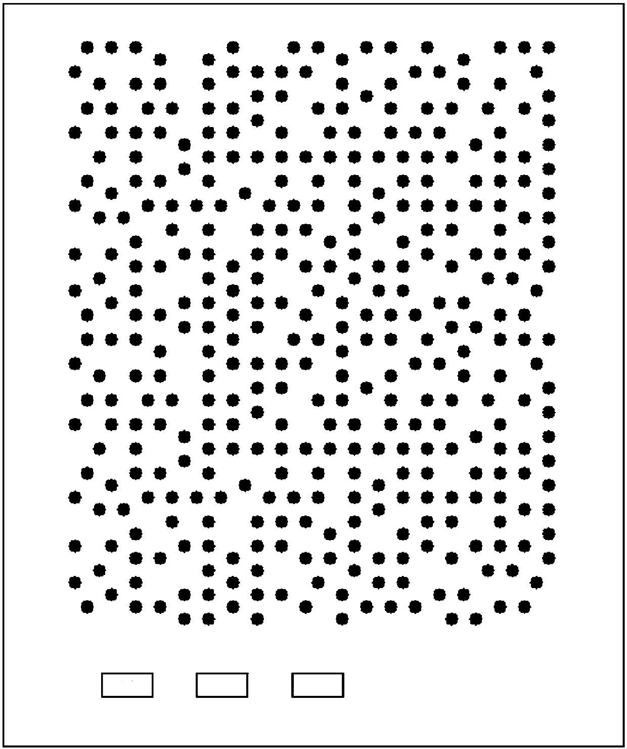
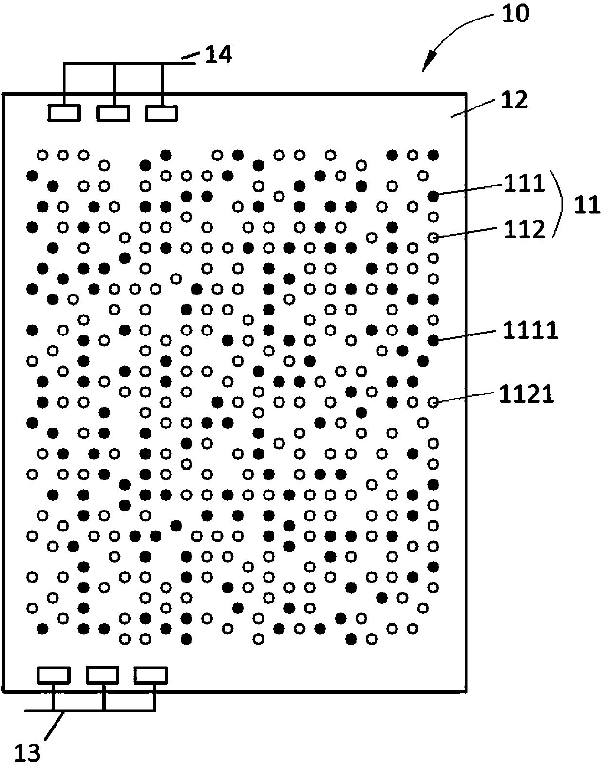
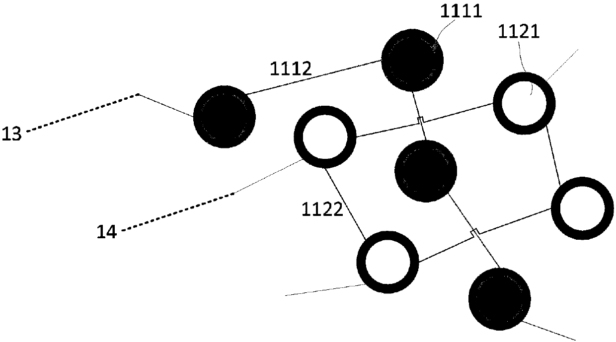
[0041] Such as figure 2 As shown, the preferred embodiment of the present invention discloses a VCSEL array 10 for a 3D depth acquisition device, including a light-emitting component 11 and a semiconductor substrate 12, and the light-emitting component 11 is distributed on the surface of the semiconductor substrate 12 in the form of a two-dimensional array; wherein The light-emitting assembly 11 includes a first group of light-emitting unit groups 111 and a second group of light-emitting unit groups 112, wherein the first group of light-emitting unit groups 111 includes a plurality of first light-emitting units 1111 that are connected to each other, and the second group of light-emitting unit groups 112 includes multiple The first group of light emitting unit groups 111 and the second group of light emitting unit groups 112 ...


PUM


Abstract

The invention discloses a VCSEL array for a 3D depth acquisition device. The VCSEL array comprises light-emitting assemblies and a semiconductor substrate, and the light-emitting assemblies are distributed on the surface of the semiconductor substrate and comprise at least two light-emitting unit groups, wherein each light-emitting unit group comprises a plurality of light-emitting units which arecommunicated with one another, the light-emitting unit groups are distributed on the semiconductor substrate in a mutually staggered manner according to the respective corresponding patterns, and thepatterns corresponding to the light-emitting assemblies formed by the patterns corresponding to the light-emitting unit groups are irregular patterns. The 3D depth acquisition device is provided withat least two groups of wires, and each group of wires is connected with and is used for driving each light-emitting unit group. The invention also discloses a processing method of the VCSEL array andthe 3D depth acquisition device. According to the present invention, the depth precision and the energy consumption obtained in specific 3D application can be well balanced.

Description

technical field [0001] The present invention relates to the field of 3D depth acquisition equipment, in particular to a VCSEL array used for 3D depth acquisition equipment and the 3D depth acquisition equipment. Background technique [0002] 3D depth technology is gradually entering the field of mass consumption. Common technologies include binocular stereo matching, ToF (time of flight) and structured light. Especially structured light technology, which can work in weak texture areas, has high precision and reasonable energy consumption, so it is more and more favored by people. The core component of structured light is the laser projection module, which projects a series of patterns onto the object, while the imaging optical module captures the patterns projected onto the object, and processes the patterns through the processor to obtain the 3D depth information of the object. [0003] As VCSEL (Vertical Cavity Surface Emitting Laser) technology is becoming more and more ...

Claims


Application Information

Patent Timeline
IPC IPC(8): H01S5/183
CPCH01S5/183
Inventor 蒋建华
Owner 深圳市安思疆科技有限公司
Why Eureka
Try Eureka