Millimeter wave frequency band amplifier chip packaging structure and manufacturing method thereof

A chip packaging structure, millimeter-wave frequency band technology, applied in semiconductor/solid-state device manufacturing, electric solid-state devices, semiconductor devices, etc., can solve the problems of high loss of millimeter-wave amplifiers, difficulty in exerting superior performance, etc., to shorten the connection length and improve the performance. Its own RF performance and the effect of reducing parasitic inductance

Pending Publication Date: 2020-01-31
NORTH-CHINA INTEGRATED CIRCUIT CO LTD
View PDF0 Cites 31 Cited by
  • Summary
  • Abstract
  • Description
  • Claims
  • Application Information

AI Technical Summary

Problems solved by technology

[0004] The purpose of the present invention is to provide a millimeter-wave frequency band amplifier chip package structure and a method for making the package structure, so as to solve the technical problem that the plastic package structure in the prior art is likely to cause excessive loss of the millimeter-wave amplifier and make it difficult to exert its superior performance

Method used


Image

  • Millimeter wave frequency band amplifier chip packaging structure and manufacturing method thereof
  • Millimeter wave frequency band amplifier chip packaging structure and manufacturing method thereof
  • Millimeter wave frequency band amplifier chip packaging structure and manufacturing method thereof

Examples


Embodiment Construction

[0030] In order to make the technical problems, technical solutions and beneficial effects to be solved by the present invention clearer, the present invention will be further described in detail below in conjunction with the accompanying drawings and embodiments. It should be understood that the specific embodiments described here are only used to explain the present invention, not to limit the present invention.

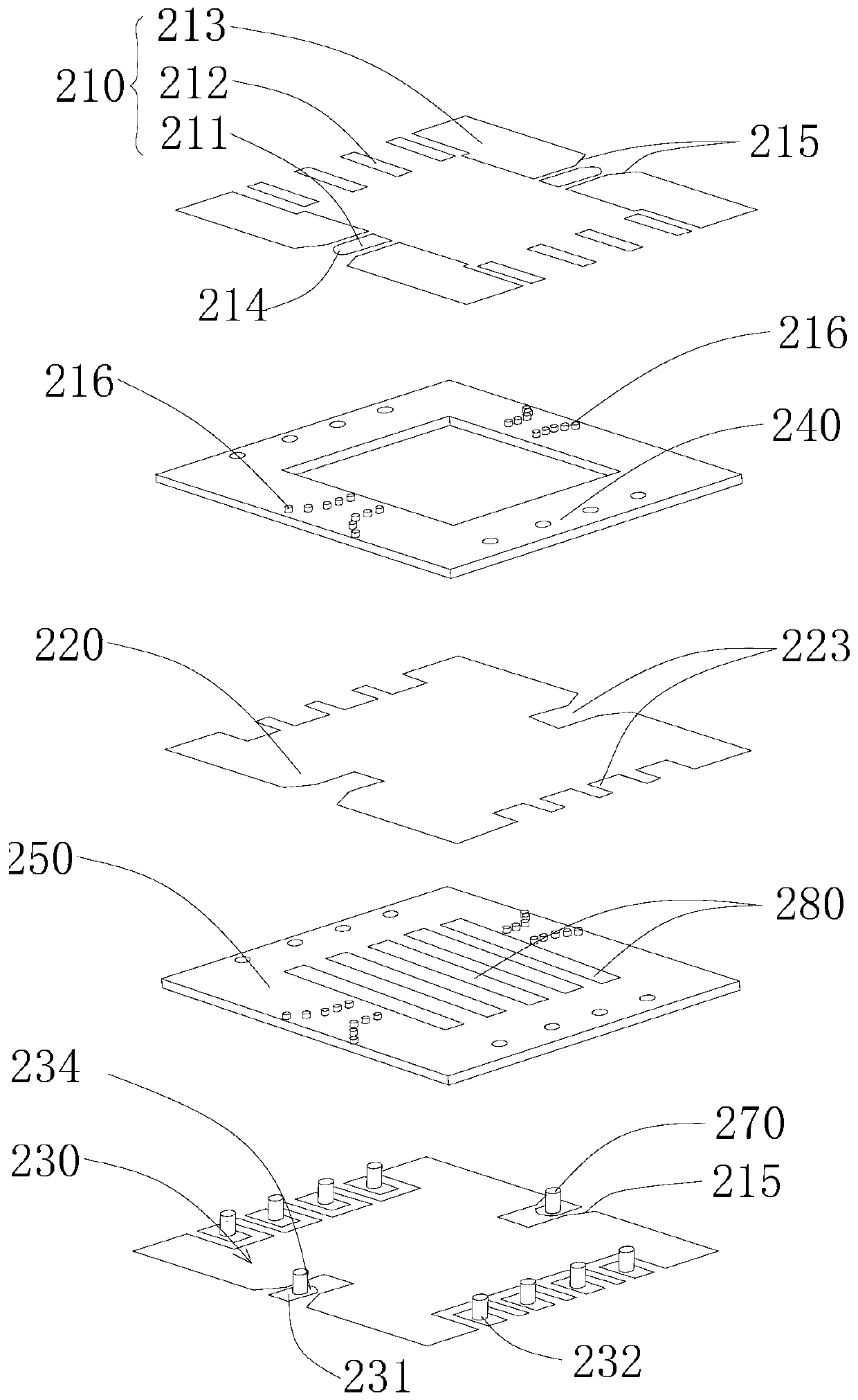
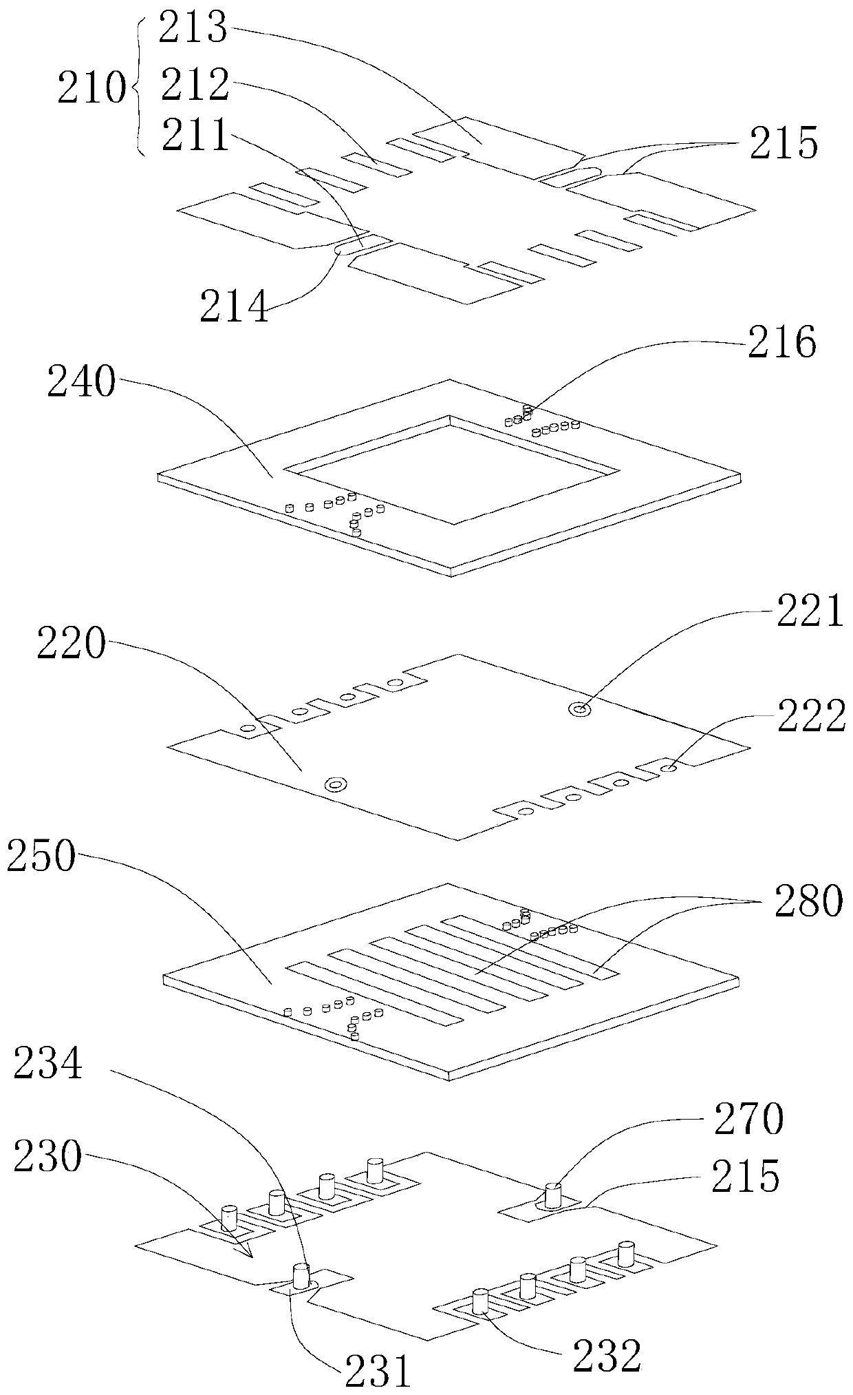
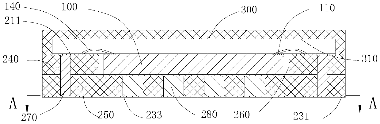
[0031] Please also refer to Figure 1 to Figure 7 Now, the packaging structure of the millimeter wave amplifier chip provided by the present invention and the method for manufacturing the packaging structure will be described. It includes a chip 100, a packaging substrate and a cover 300; several chip DC ports 120 and two chip RF ports 110 are provided on the upper surface of the chip 100; layer 210 , first dielectric layer 240 , second metal layer 220 , second dielectric layer 250 and third metal layer 230 . The middle part of the first metal layer 210 and the f...


PUM


Abstract

The invention provides a millimeter wave frequency band amplifier chip packaging structure and a manufacturing method thereof and relates to the technical field of chip packaging. The structure comprises a chip, a packaging substrate and a sealing cover, wherein the packaging substrate is provided with a first metal layer, a first dielectric layer, a second metal layer, a second dielectric layer and a third metal layer which are sequentially stacked from top to bottom, the sealing cover is arranged on the packaging substrate and used for sealing the packaging substrate, and the sealing cover is provided with an inner cavity with a downward opening. The millimeter wave frequency band amplifier chip packaging structure is advantaged in that the packaging substrate and the sealing cover are combined, an accommodating groove is formed in the packaging substrate so that the chip is accommodated, the connection length between the chip and the packaging substrate is effectively shortened, theparasitic inductance is conveniently reduced, and the transmission capability of the chip is improved; the sealing cover with the inner cavity enables connection between a chip direct-current port ofthe chip and the packaging substrate to be in direct contact with air, so loss of a high-frequency band is reduced, and radio frequency performance of the chip is improved.

Description

technical field [0001] The invention belongs to the technical field of chip packaging, and more specifically relates to a millimeter-wave frequency band amplifier chip packaging structure and a method for manufacturing the packaging structure. Background technique [0002] With the development of millimeter wave frequency band technology, millimeter wave communication technology is widely used in mobile communication, radar detection, electronic countermeasures, precision guidance and other fields. Amplifier chips in the millimeter wave band generally adopt the design of monolithic microwave integrated circuits, which have the advantages of good microwave performance and high integration. [0003] At present, most microwave radio frequency chips use plastic encapsulation technology. In this process, the metal package carrier frame is firstly made, and then the chip is bonded on the frame, the chip is bonded to the package pin, the chip injection is completed through the inj...

Claims


Application Information

Patent Timeline
Patent Type & Authority Applications(China)
IPC IPC(8): H01L23/495H01L21/48
CPCH01L21/4853H01L23/4952H01L23/49548H01L23/49568H01L2224/05554H01L2224/48091H01L2224/49171H01L2224/73265H01L2924/00014
Inventor 张晓朋吴兰高博曲韩宾邢浦旭崔培水谷江
Owner NORTH-CHINA INTEGRATED CIRCUIT CO LTD
Why Eureka
Try Eureka