Display device and its oled light-transmitting substrate, oled substrate

A technology of light-transmitting substrate and base color, applied in semiconductor devices, electrical components, circuits, etc., can solve problems such as affecting the overall consistency of the screen

Active Publication Date: 2022-03-01
KUNSHAN GO VISIONOX OPTO ELECTRONICS CO LTD
View PDF6 Cites 0 Cited by
  • Summary
  • Abstract
  • Description
  • Claims
  • Application Information

AI Technical Summary

Problems solved by technology

[0002] With the rapid development of display devices, users have higher and higher requirements for screen-to-body ratio. Since cameras, sensors, earpieces and other components need to be installed above the screen, a part of the area above the screen is usually reserved in the prior art for the installation of the above-mentioned Components, such as the front notch area of ​​the iPhone X, affect the overall consistency of the screen, and the full-screen display has attracted more and more attention from the industry

Method used


Image

  • Display device and its oled light-transmitting substrate, oled substrate
  • Display device and its oled light-transmitting substrate, oled substrate
  • Display device and its oled light-transmitting substrate, oled substrate

Examples


Embodiment Construction

[0094] In order to make the above objects, features and advantages of the present invention more comprehensible, specific embodiments of the present invention will be described in detail below in conjunction with the accompanying drawings.

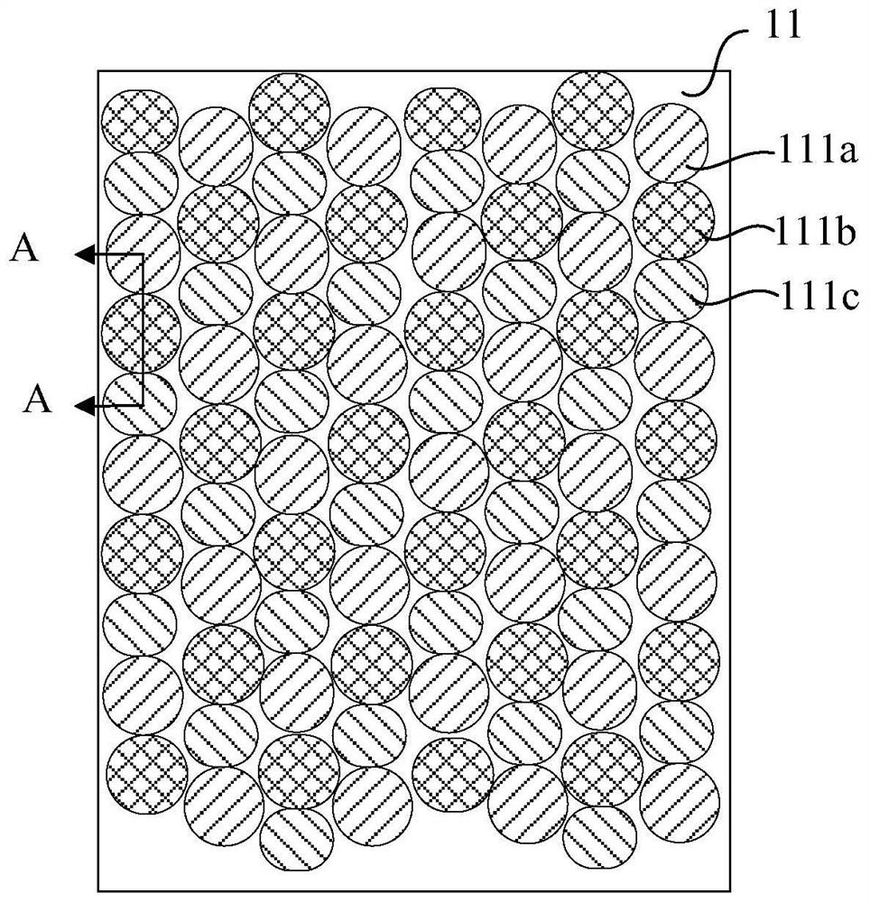
[0095] figure 1 It is a top view of the OLED light-transmitting substrate in the first embodiment of the present invention. figure 2 is along figure 1 Sectional view of line AA in .

[0096] refer to figure 1 and figure 2 As shown, the OLED light-transmitting substrate 11 includes:

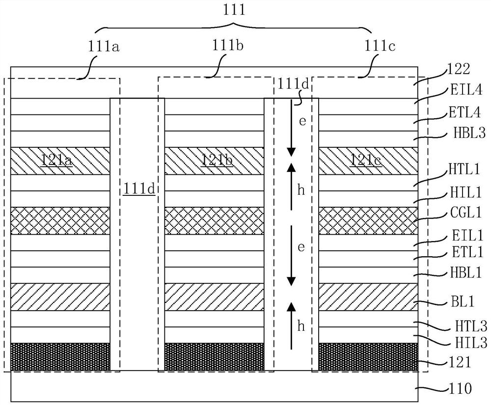
[0097] The light-transmitting base 110 and the arrayed light-emitting units 111 located on the light-transmitting base 110, each light-emitting unit 111 includes several sub-light-emitting structures 111a, 111b, 111c, and each sub-light-emitting structure 111a, 111b, 111c includes from bottom to top: A light-transmitting anode 121, luminescent material layers 121a, 121b, 121c corresponding to primary colors, and a light-transmitting cathode 122;

[009...


PUM

PropertyMeasurementUnit
electron work functionaaaaaaaaaa
thicknessaaaaaaaaaa
thicknessaaaaaaaaaa

Abstract

The invention provides a display device and its OLED light-transmitting substrate, and the OLED substrate. For the OLED light-transmitting substrate, a second light-emitting anode is sandwiched from bottom to top between the light-transmitting anode of at least one sub-light-emitting structure and the light-emitting material layer corresponding to the primary color. An illuminating material layer and a first charge generating layer; and / or a second charge generating layer and a second illuminating layer are sandwiched from bottom to top between the light-transmitting cathode of at least one sub-luminescent structure and the luminescent material layer corresponding to the primary color. material layer. The advantage is that electrons and holes are respectively provided to the first illuminating material layer and the luminescent material layer corresponding to the primary color through the first charge generating layer, and / or the second illuminating material layer and the corresponding primary color are provided through the second charge generating layer. The luminescent material layer provides electrons and holes respectively, so that the composite luminescence of electrons and holes in at least one of the first illuminating material layer and the second illuminating material layer can improve the luminous brightness of the luminescent material layer corresponding to the primary color, thereby Improve the brightness and life of the transparent display area.

Description

technical field [0001] The invention relates to the technical field of OLED display equipment, in particular to a display device and its OLED light-transmitting substrate and OLED substrate. Background technique [0002] With the rapid development of display devices, users have higher and higher requirements for screen-to-body ratio. Since cameras, sensors, earpieces and other components need to be installed above the screen, a part of the area above the screen is usually reserved in the prior art for the installation of the above-mentioned Components, such as the front notch area of ​​the iPhone X, affect the overall consistency of the screen, and the full-screen display has attracted more and more attention from the industry. Contents of the invention [0003] The object of the present invention is to provide a display device and its OLED light-transmitting substrate and OLED substrate, so as to improve the brightness and lifespan of the transparent display area. [000...

Claims


Application Information

Patent Timeline
Patent Type & Authority Patents(China)
IPC IPC(8): H01L27/32
CPCH10K59/35
Inventor 葛林楼均辉蔡世星
Owner KUNSHAN GO VISIONOX OPTO ELECTRONICS CO LTD
Why Eureka
Try Eureka