Liquid crystal display device and liquid crystal display device manufacturing method thereof

A technology of a liquid crystal display device and a manufacturing method, which is applied in nonlinear optics, instruments, optics, etc., and can solve problems such as high manufacturing cost, serious brightness loss, and difficulty in meeting use requirements

Active Publication Date: 2020-02-11
KUSN INFOVISION OPTOELECTRONICS
View PDF5 Cites 3 Cited by
  • Summary
  • Abstract
  • Description
  • Claims
  • Application Information

AI Technical Summary

Problems solved by technology

In order to protect commercial secrets and personal privacy, shutter technology can be used, but this technology cannot be switched to wide viewing angle mode, and the brightness loss is serious. At the same time, the manufacturing cost is high, and it is difficult to meet the use requirements.

Method used


Image

  • Liquid crystal display device and liquid crystal display device manufacturing method thereof
  • Liquid crystal display device and liquid crystal display device manufacturing method thereof
  • Liquid crystal display device and liquid crystal display device manufacturing method thereof

Examples


no. 1 example

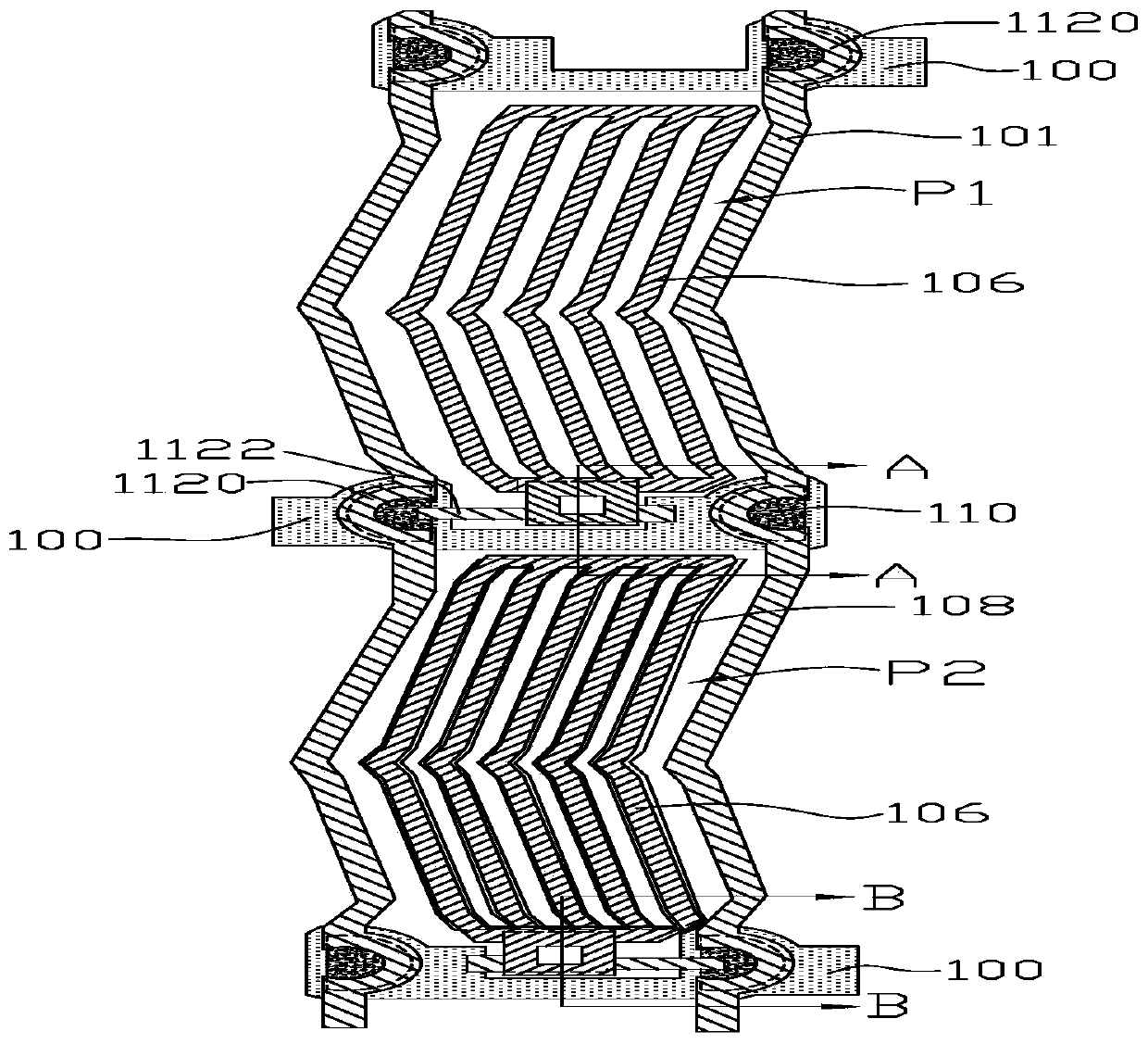
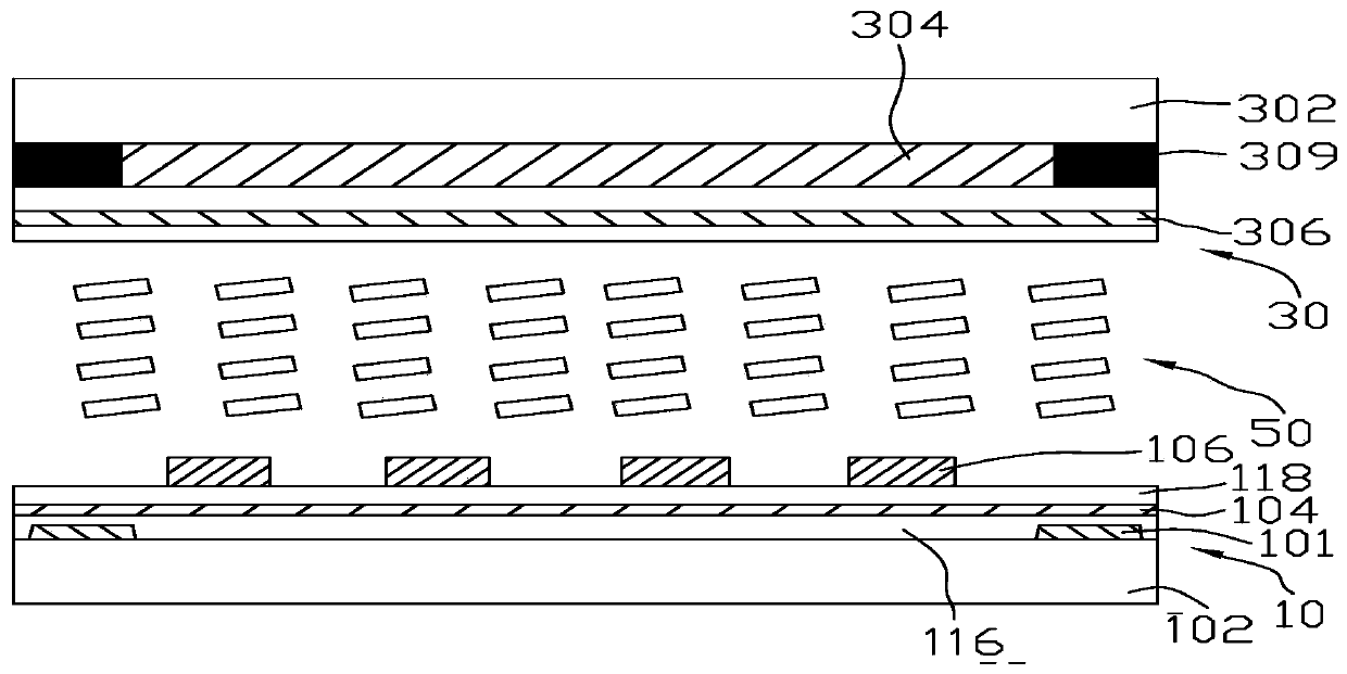
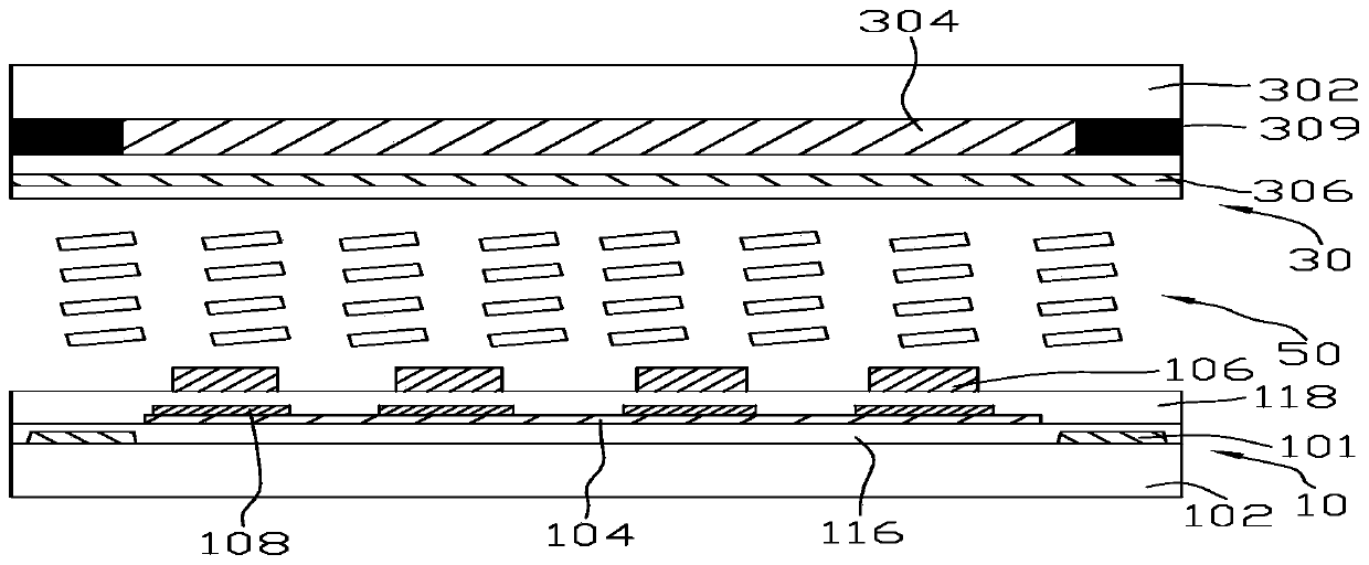
[0028] Such as Figure 1 to Figure 3 As shown, the liquid crystal display device according to the first embodiment of the present invention includes an array substrate 10 , a color filter substrate 30 opposite to the array substrate 10 , and a liquid crystal layer 50 located between the array substrate 10 and the color filter substrate 30 . A plurality of first pixel units P1 and a plurality of second pixel units P2 are formed on the array substrate 10 defined by the scan lines 100 and the data lines 101 . The array substrate 10 includes a first substrate 102 , a thin film transistor, a first conductive layer 104 , a second conductive layer 106 and a shielding layer 108 . The first conductive layer 104 is disposed above the TFT, the second conductive layer 106 is separated from the first conductive layer 104 , and the shielding layer 108 is disposed between the first conductive layer 104 and the second conductive layer 106 . The shielding layer 108 is disposed in the region c...

no. 2 example

[0041] Please refer to Figure 11 and Figure 12 The structure of the liquid crystal display device of the second embodiment of the present invention is basically the same as that of the liquid crystal display device of the first embodiment. area, and set on the color filter substrate 30 . More specifically, the shielding layer 108 is disposed on a side of the color filter substrate 30 close to the liquid crystal layer 50 . The shielding layer 108 is disposed corresponding to the second common electrode in the second pixel unit P2. Other structures of the liquid crystal display device of this embodiment are similar to those of the liquid crystal display device of the first embodiment, and the driving method is also similar, so details will not be repeated here.

no. 3 example

[0043] Please refer to Figure 13 and Figure 14, the structure of the liquid crystal display device of the third embodiment of the present invention is basically the same as that of the liquid crystal display device of the second embodiment, the difference is that in the third embodiment, the first conductive layer 104 is in the first pixel unit P1 The first common electrode is formed in the second pixel unit P2, the second common electrode is formed in the second pixel unit P2, the second conductive layer 106 forms the first pixel electrode in the first pixel unit P1, and the second pixel electrode is formed in the second pixel unit P2 . The shielding layer 108 is disposed corresponding to the area between adjacent second pixel electrodes. The shielding layer 108 is disposed in a region corresponding to the second pixel unit P2 and disposed on the color filter substrate 30 . More specifically, the shielding layer 108 is disposed on a side of the color filter substrate 30 ...


PUM


Abstract

The invention discloses a liquid crystal display device and a liquid crystal display device manufacturing method. The liquid crystal display device comprises an array substrate, a color film substrateand a liquid crystal layer, wherein a plurality of first pixel units and a plurality of second pixel units are formed on the array substrate, the array substrate comprises a shielding layer, and theshielding layer is arranged in an region corresponding to the second pixel units and used for shielding front viewing angle light leakage during full-narrow viewing angle display of the liquid crystaldisplay device; the color film substrate comprises a third conducting layer, and the third conducting layer is a visual angle control electrode. According to the liquid crystal display device manufactured by means of the liquid crystal display device manufacturing method, wide viewing-angle display, full-narrow viewing-angle display and left-right narrow-viewing-angle display can be achieved, left-right peep prevention and up-down peep prevention can be achieved simultaneously in a full-narrow viewing-angle mode, and the peep prevention effect is greatly improved; the shielding layer can shield part of light leakage at a front viewing angle, and can prevent light leakage at the front viewing angle in a full-narrow viewing angle mode, so that large-viewing-angle light leakage is achieved,the front-viewing-angle light leakage is avoided or reduced and the display effect is improved.

Description

technical field [0001] The invention relates to the technical field of liquid crystal display, in particular to a liquid crystal display device and a method for manufacturing the liquid crystal display device. Background technique [0002] Liquid crystal display devices have the advantages of good image quality, small size, light weight, low driving voltage, low power consumption, no radiation, and relatively low manufacturing costs, and occupy a dominant position in the field of flat panel displays. With the continuous advancement of liquid crystal display technology, the viewing angle of the display has been expanded from about 120° to more than 160°. While enjoying the visual experience brought by the large viewing angle, people also hope to effectively protect commercial secrets and personal privacy. In order to avoid commercial loss or embarrassment caused by leakage of screen information. Therefore, in addition to the wide viewing angle, the display device is also req...

Claims


Application Information

Patent Timeline
IPC IPC(8): G02F1/13G02F1/1335G02F1/1343
CPCG02F1/1323G02F1/133512G02F1/134309
Inventor 沈家军吴佳星周学芹李冬敏
Owner KUSN INFOVISION OPTOELECTRONICS
Why Eureka
Try Eureka