High-density Micro LED sandwich structure active driving display unit
A sandwich structure and display unit technology, which is applied to electrical components, instruments, electric solid devices, etc., can solve the problem that it is difficult to further reduce the pixel pitch of LED display units, etc.
- Summary
- Abstract
- Description
- Claims
- Application Information
AI Technical Summary
Problems solved by technology
Method used
Image

Examples
Embodiment 1
[0051] In order to solve the problem that there will be gaps in the splicing of LED display screens using TFT display drive circuits, the present invention grows metal pillars on one side of the transparent glass carrier board with the LED flip-chip structure light-emitting chip that emits light from the reverse side, and grows metal pillars on the opposite side of the printed circuit carrier board. The metal pad pillars grown in corresponding positions are butted to lead the driving circuit to the printed circuit carrier. Taking the LED flip-chip structure light-emitting chip that emits light from the reverse side as an example, the specific technical solution of the present invention is as follows:
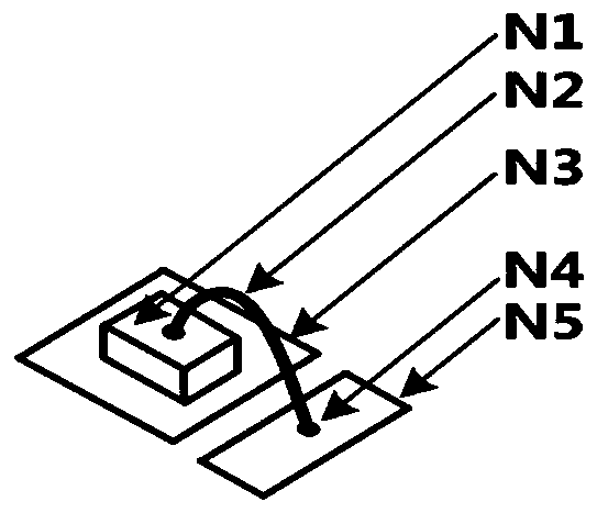
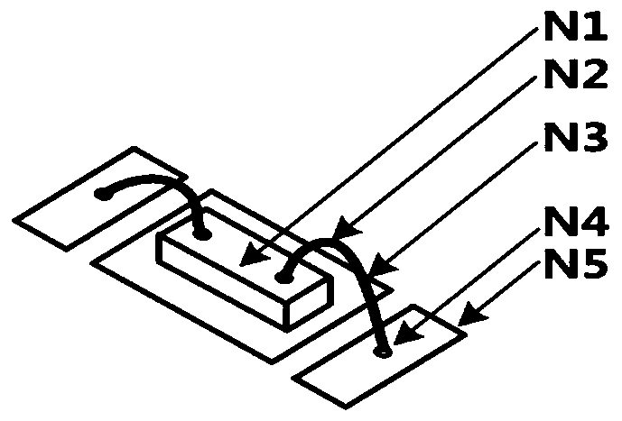
[0052] Such as Figure 5 As shown, J2 is the LED flip-chip structure light-emitting chip that emits light from the reverse side, G2 is the light-emitting surface of the LED flip-chip structure light-emitting chip J2, G is the transparent glass carrier that fixes the LED flip-chi...
Embodiment 2
[0060] In order to solve the problem that there will be gaps in the splicing of LED display screens using TFT display drive circuits, the invention fixes the LED flip-chip structure light-emitting chips on the back of the transparent glass carrier, and prints the leads on the transparent glass carrier through metal columns. The lead connections on the circuit carrier lead the drive circuit to the printed circuit carrier. Taking the LED flip-chip structure light-emitting chip that emits light from the reverse side as an example, the specific technical solution of the present invention is as follows:
[0061] Such as Figure 5 As shown, J2 is the LED flip-chip structure light-emitting chip that emits light from the reverse side, G2 is the light-emitting surface of the LED flip-chip structure light-emitting chip J2, G is the transparent glass carrier that fixes the LED flip-chip structure light-emitting chip J2, and J4 is the LED flip-chip structure The electrode of the light-em...
Embodiment 3
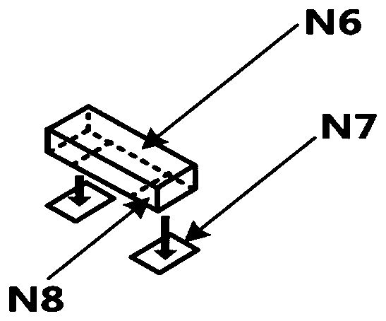
[0068] Such as Figure 13 As shown, the active driving display unit of the high-density Micro LED sandwich structure of the present invention includes a transparent glass carrier G, a printed circuit carrier B, a basic pixel unit, a TFT driving device T, and a circuit driver J20; the basic pixel unit includes The red, green and blue three-primary-color LED light-emitting chips P2, P3 and P4, and the red, green and blue three-primary-color LED light-emitting chips P2, P3 and P4 all use reverse-side LED flip-chip structure light-emitting chips, and other structural forms can also be used. The LED light-emitting chip emitting light from the reverse side; the two electrodes J4 of the LED flip-chip structure light-emitting chip are bonded to the two electrodes of the TFT driving device T through the glass carrier pad J6; the TFT driving device T is fixed on the transparent glass carrier G, It is used to drive the LED flip-chip light-emitting chip to emit light, and the TFT driving de...
PUM
 Abstract
Description
Claims
Application Information
 - R&D
- Intellectual Property
- Life Sciences
- Materials
- Tech Scout
- Unparalleled Data Quality
- Higher Quality Content
- 60% Fewer Hallucinations
Browse by: Latest US Patents, China's latest patents, Technical Efficacy Thesaurus, Application Domain, Technology Topic, Popular Technical Reports.
© 2025 PatSnap. All rights reserved.Legal|Privacy policy|Modern Slavery Act Transparency Statement|Sitemap|About US| Contact US: help@patsnap.com