Supercharge Your Innovation With Domain-Expert AI Agents!

Flash memory device and manufacturing method thereof

A technology for flash memory devices and manufacturing methods, which is applied in the direction of electric solid-state devices, semiconductor devices, electrical components, etc., which can solve the problems of fast speed and slow read and write speed, and achieve the effects of avoiding defects, improving uniformity, and reducing production costs

Active Publication Date: 2020-02-14
WUHAN XINXIN SEMICON MFG CO LTD
View PDF3 Cites 0 Cited by
  • Summary
  • Abstract
  • Description
  • Claims
  • Application Information

AI Technical Summary

Problems solved by technology

Non-volatile memory devices include NAND and NOR flash memory (Flash Memory) types, of which NAND flash memory has a large storage capacity, but the read and write speed is slow, while NOR flash memory is faster

Method used


Image

  • Flash memory device and manufacturing method thereof
  • Flash memory device and manufacturing method thereof
  • Flash memory device and manufacturing method thereof

Examples


Embodiment Construction

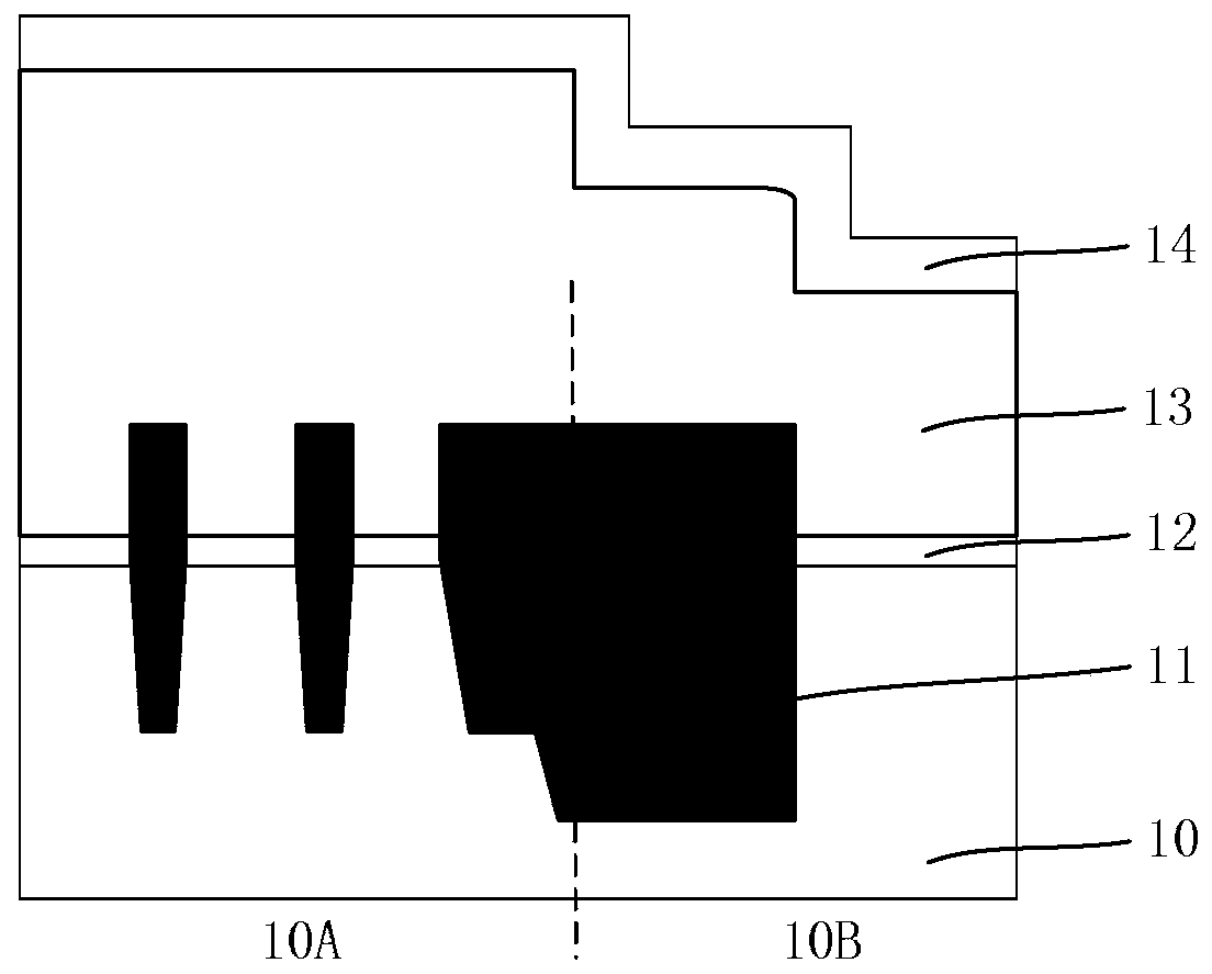
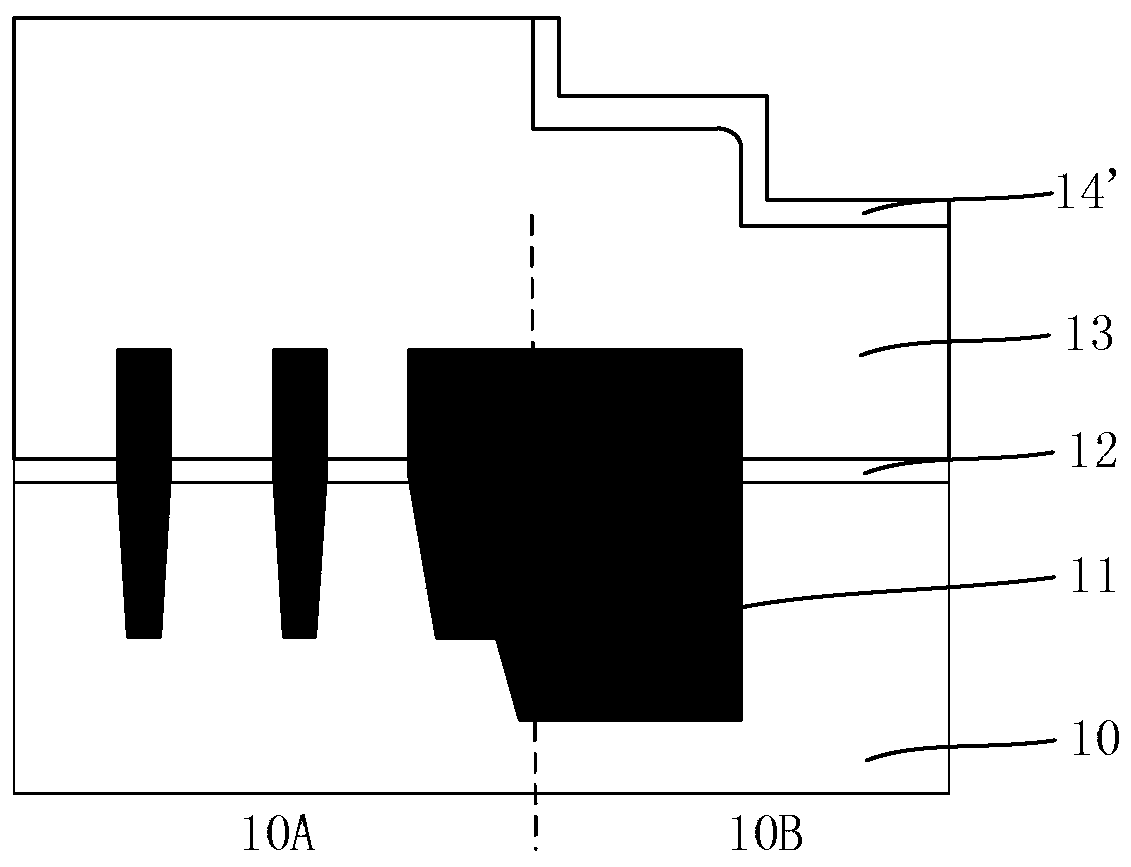
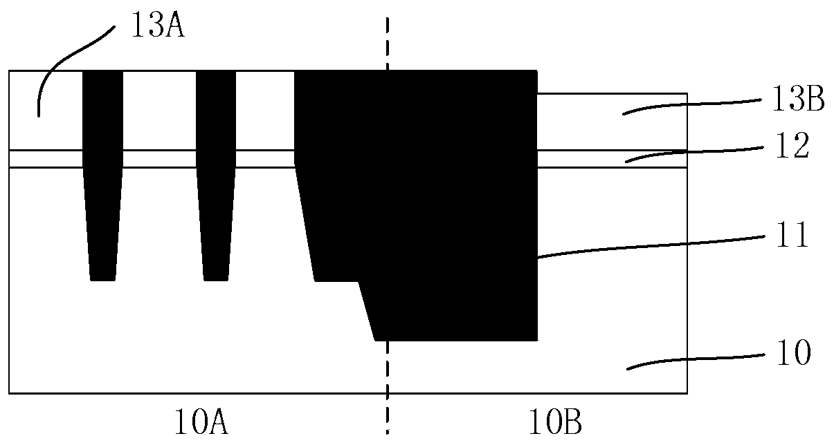
[0036] Figure 1-6 It is a structural schematic diagram of each step of a manufacturing method of a flash memory device. Please refer to Figure 1 to Figure 6 As shown, the fabrication method of the flash memory device is as follows.

[0037] First, please refer to figure 1 As shown, a substrate 10 is provided, the substrate 10 includes a storage area 10A and a peripheral area 10B, a plurality of isolation structures 11 are formed in the substrate 10, and the upper surface of the isolation structures 11 is higher than the the upper surface of the substrate 10. A gate dielectric layer 12 is formed on the substrate 10 . Similarly, the upper surface of the isolation structure 11 is higher than the upper surface of the gate dielectric layer 12 . The material of the isolation structure 11 is preferably silicon oxide, and the material of the gate dielectric layer 12 is preferably silicon oxide.

[0038] Next, a floating gate material layer 13 is formed on the gate dielectric la...


PUM

PropertyMeasurementUnit
Thicknessaaaaaaaaaa
Thicknessaaaaaaaaaa

Abstract

The invention provides a flash memory device and a manufacturing method thereof. An oxide layer is formed on a floating gate material layer; after the oxide layer and the floating gate material layerare flattened, the remaining floating gate material layer in a storage region forms floating gates, and part of the floating gate material layer in the thickness direction is reserved in the peripheral region; and isolation structures between the floating gates are etched by taking the floating gates and part of the floating gate material layer in the thickness direction reserved in the peripheralregion as masks. A patterning process can be saved, defects caused by photoresist patterning are avoided, the production cost is reduced, and the uniformity of the floating gates is improved.

Description

technical field [0001] The invention relates to the technical field of semiconductor manufacturing, in particular to a flash memory device and a manufacturing method thereof. Background technique [0002] Generally speaking, semiconductor memory used to store data is divided into volatile memory and nonvolatile memory. Volatile memory is prone to data loss when power is interrupted, while nonvolatile memory The internal information of the memory can still be saved in time after being closed, and the non-volatile memory device has the characteristics of low cost and high density, so that the non-volatile memory device is widely used in various fields. Non-volatile memory devices include NAND and NOR flash memory (Flash Memory) types, of which NAND flash memory has a large storage capacity, but the read and write speed is slow, while NOR flash memory is Faster. [0003] As the size of the Nor Flash process continues to decrease, the requirements for the uniformity of the flo...

Claims


Application Information

Patent Timeline
IPC IPC(8): H01L27/11517H01L27/11521H01L21/28
CPCH10B41/00H10B41/30
Inventor 薛广杰胡华李赟
Owner WUHAN XINXIN SEMICON MFG CO LTD
Features
  • R&D
  • Intellectual Property
  • Life Sciences
  • Materials
  • Tech Scout
  • Unparalleled Data Quality
  • Higher Quality Content
  • 60% Fewer Hallucinations
Learn More