PCB connecting structure

A connection structure and hinged technology, applied in the structural connection of printed circuits, printed circuit components, electrical components, etc., can solve the problem of increasing PCB manufacturing costs, reducing the structural strength of PCB boards, affecting the overall structural strength of PCB boards and connectors, etc. problems, to achieve the effects of reducing production costs, retaining structural strength, and wide adaptability

Pending Publication Date: 2020-02-14
AOSHIKANG TECH CO LTD
View PDF1 Cites 0 Cited by
  • Summary
  • Abstract
  • Description
  • Claims
  • Application Information

AI Technical Summary

Problems solved by technology

Before each connection, corresponding two rows of jacks need to be drilled on the PCB, and the pins on the connector are inserted into the jacks for connection. This design will increase the manufacturing cost of the PCB. Secondly, the drilling will reduce the cost of the PCB. Structural strength, affecting the overall structural strength of PCB boards and connectors

Method used


Image

  • PCB connecting structure
  • PCB connecting structure
  • PCB connecting structure

Examples


Embodiment Construction

[0021] In order to make the object, technical solution and advantages of the present invention clearer, the present invention will be further described in detail below in conjunction with the accompanying drawings and embodiments. It should be understood that the specific embodiments described here are only used to explain the present invention, not to limit the present invention.

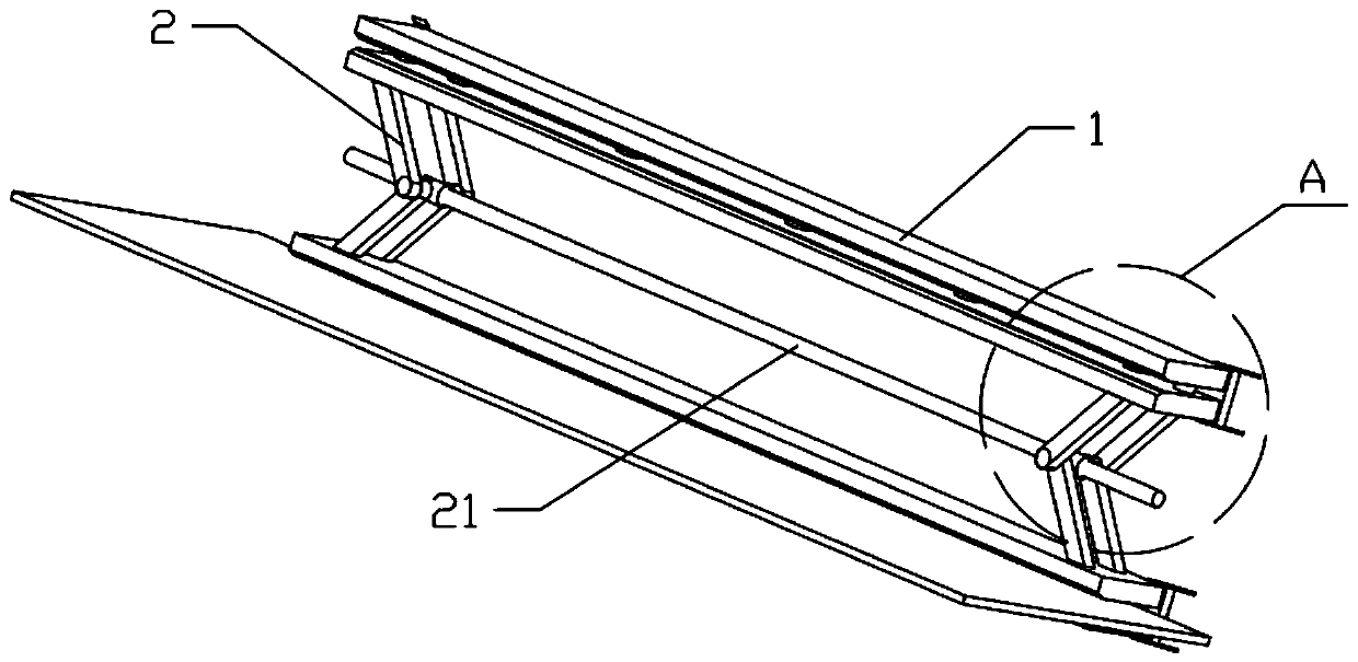
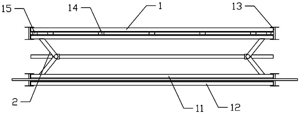
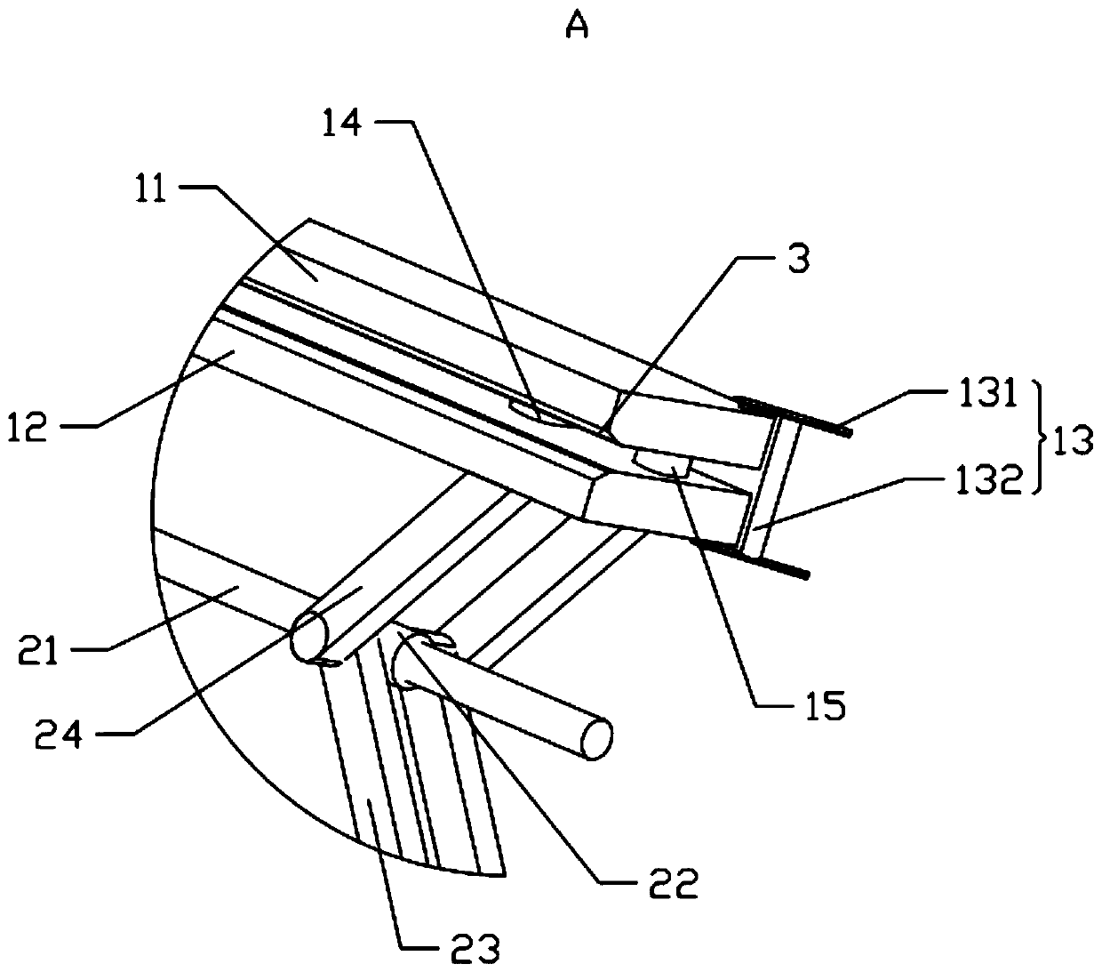
[0022] Refer to attached Figure 1-3 , the present embodiment includes two opposite clamps 1, a height adjustment assembly 2 is arranged between the two clamps 1, and the height adjustment assembly 2 is respectively hinged with the two clamps 1; the clamp 1 includes an upper splint 11 and a lower splint 12, the upper A sliding group and a spring group are provided between the clamping plate 11 and the lower clamping plate 12, so that the upper clamping plate 11 and the lower clamping plate 12 are opened or clamped along the height direction, and the two ends of the clamp 1 are provided with clips 1...


PUM


Abstract

A PCB connecting structure comprises two clamps which are oppositely arranged. A height adjusting assembly is arranged between the two clamps, and the height adjusting assembly is hinged to the two clamps. Each clamp comprises an upper clamping plate and a lower clamping plate, and a sliding set and a spring set are arranged between the upper clamping plate and the lower clamping plate, so that the upper clamping plate and the lower clamping plate can be opened or clamped in the height direction. Clips are arranged at the two ends of the clamps, the clips are rotationally connected with the upper clamping plates and the lower clamping plates, and the clips, the sliding set and the spring set are all arranged along one long edge of each upper clamping plate. Compared with the prior art, twoPCBs can be conveniently and quickly connected. The clamps can clamp PCBs longer than the clamps and PCBs shorter than the clamps, and the adaptability is high. Through the arrangement of the heightadjusting assembly, the height between the clamps can be conveniently adjusted to enable the structure to adapt to more PCBs. Because of the design, PCBs do not need to be specially processed, the original structural strength of the PCBs is kept, and the manufacturing cost of the PCBs is reduced.

Description

technical field [0001] The invention relates to the technical field of PCB board manufacturing, in particular to a PCB connection structure. Background technique [0002] With the development of science and technology, the integration of controllers is getting higher and higher and the modularization is becoming more and more frequent. In many drive and control integrated products, there are usually several PCB boards that are connected together, and board-to-board connectors are often required. The patent with the publication number CN209389248U discloses a PCB board connector, which consists of a PCB adapter board and pin headers. The pin headers are arranged on the upper and / or lower ends of the PCB adapter board. The upper and lower ends of the PCB adapter board / or the lower end is provided with at least two rows of upper and lower rows of parallel pin jacks, and the end of the PCB adapter board is provided with positioning columns parallel to the pin headers, and the h...

Claims


Application Information

Patent Timeline
IPC IPC(8): H05K1/14
CPCH05K1/144
Inventor 程文君雷刚
Owner AOSHIKANG TECH CO LTD
Why Eureka
Try Eureka