Huge amount interval adjusting method and huge amount transferring method and equipment of tiny electronic components

A technology of electronic components and adjustment methods, applied in the direction of conveyor objects, transportation and packaging, etc., can solve the problems of Micro-LED centrifugal dispersion deviation, difficulty in ensuring no adhesion, deviation of centrifugal dispersion results, etc., to achieve convenient function realization , Easy and precise decentralized control, low rate of out of control effect

Active Publication Date: 2020-02-21
颜色空间(北京)科技有限公司
View PDF6 Cites 2 Cited by
  • Summary
  • Abstract
  • Description
  • Claims
  • Application Information

AI Technical Summary

Problems solved by technology

[0007] 1. Placing Micro-LED chips on a rubber carrier can increase friction, but Micro-LED devices are extremely small and light, and it is difficult to ensure that some devices in a huge Micro-LED array do not stick to the rubber sheet when placed on a rubber carrier , placed on the rubber carrier sheet will easily lead to deviations when some Micro-LEDs are centrifugally dispersed
[0008] 2. The lifting action is carried out while the dispersion platform is rotating. The rotation and lifting action need to be precisely coordinated, and the control is complicated. Improper coordination will easily lead to deviations in the centrifugal dispersion results.
[0009] 3. Micro-LED devices are extremely small and light, and it is difficult to achieve uniform air blowing on the bearing surface of the rubber carrier sheet. As long as there is a slight difference in air blowing for a large number of Micro-LED devices, the distribution will be deviated

Method used


Image

  • Huge amount interval adjusting method and huge amount transferring method and equipment of tiny electronic components
  • Huge amount interval adjusting method and huge amount transferring method and equipment of tiny electronic components
  • Huge amount interval adjusting method and huge amount transferring method and equipment of tiny electronic components

Examples


Embodiment Construction

[0038] In order to make the technical problems, technical solutions and advantages to be solved by the present invention clearer, the following will describe in detail with reference to the drawings and specific embodiments.

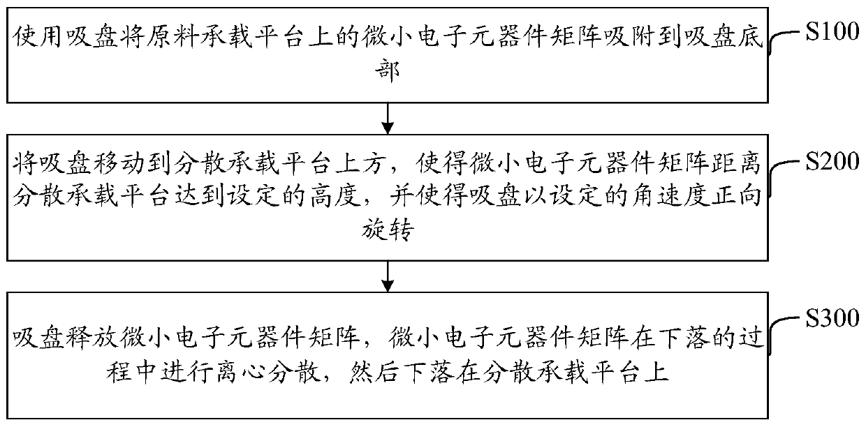
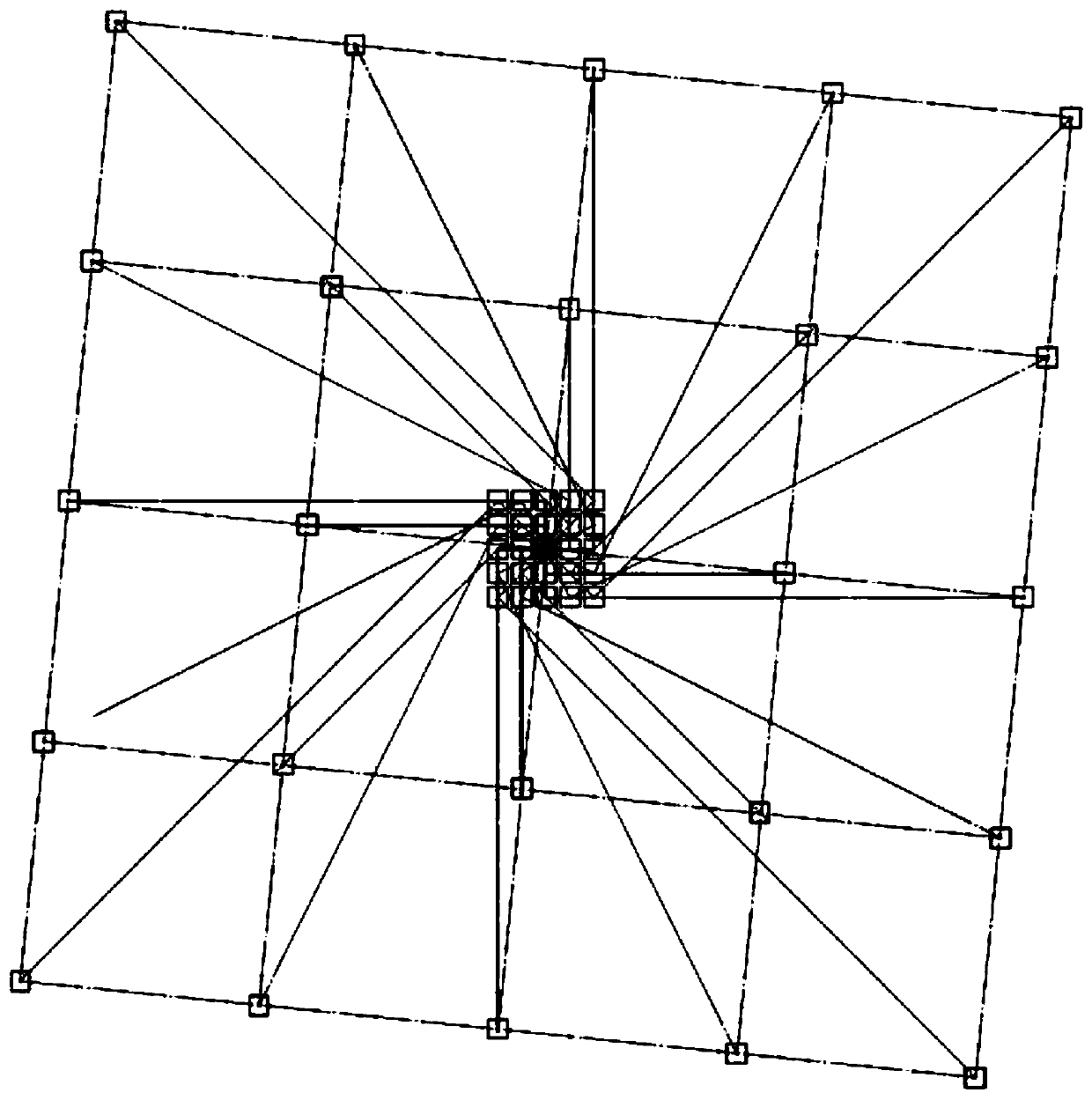
[0039] An embodiment of the present invention provides a method for adjusting a large amount of spacing between tiny electronic components, such as figure 1 As shown, the method includes:

[0040] Step S100: using a suction cup to absorb the array of tiny electronic components on the material carrying platform to the bottom of the suction cup.

[0041] Before the huge amount of pitch adjustment, the tiny electronic components are carried on the raw material carrying platform in an array. Taking Micro-LED as an example, Micro-LED chips are distributed on the wafer in an array, and the wafer is placed on the raw material carrying platform, and the array of Micro-LED chips on the wafer can be adsorbed by a suction cup.

[0042] The present invention does ...


PUM


Abstract

The invention discloses a huge amount interval adjusting method and a huge amount transferring method and equipment of tiny electronic components, and belongs to the field of the tiny electronic components. The method includes the steps that S100, tiny electronic component arrays on a raw material bearing platform are adsorbed at the bottoms of suckers through the suckers; S200, the suckers are moved above a dispersion bearing platform, the distances between the tiny electronic component arrays and the dispersion bearing platform reach the set height, and the suckers rotate forwards at a set angular speed; and S300, the tiny electronic component arrays are released by the suckers, and the tiny electronic components are centrifugally dispersed in the falling process and then fall on the dispersion bearing platform. Huge amount dispersion and huge amount interval adjustment are achieved through centrifugal dispersion, the yield is high, the out-of-control rate is low, and precise dispersion control is easily achieved.

Description

technical field [0001] The invention relates to the field of tiny electronic components, in particular to a method for adjusting a huge amount of space between tiny electronic components, a method for mass transfer and equipment. Background technique [0002] Micro-LED not only has the advantages of LCD and OLED, but also has better display performance than LCD and OLED. For example, the brightness of Micro-LED is above 100,000 lux and the service life is about 80,000-100,000 hours. Based on the advantages of Micro-LEDs that fully surround LCD and OLED, it can be expected that Micro-LEDs will be ubiquitous in the future, ranging from foldable devices, AR / VR, to 146-inch video walls, all of which are Micro-LED application scenarios. [0003] In order to realize the application of Micro-LED, it is necessary to transfer a large number (tens of thousands to tens of millions) of Micro-LED chips on the wafer to the driving circuit board to form a three-color mixed LED array with a...

Claims


Application Information

Patent Timeline
Patent Type & Authority Applications(China)
IPC IPC(8): B65G47/91B65G47/26
CPCB65G47/26B65G47/91
Inventor 陈听
Owner 颜色空间(北京)科技有限公司
Why Eureka
Try Eureka