Touch substrate and display device

A substrate and touch technology, applied in instruments, computing, electrical and digital data processing, etc., can solve the problems of abnormal touch point detection, weak current capability, and reduced mutual capacitance change.

Active Publication Date: 2020-03-06
BOE TECH GRP CO LTD
View PDF9 Cites 13 Cited by
  • Summary
  • Abstract
  • Description
  • Claims
  • Application Information

AI Technical Summary

Problems solved by technology

[0003] However, as the thickness of the module stack structure becomes thinner, the mutual capacitive touch structure is prone to abnormal touch point detection in the case of low ground mass (LGM)
Specifically, in the case of weak grounding, the capacitance formed between the finger and the ground is very small, and the current passing capacity of this path is very weak, resulting in a decrease in the mutual capacitance change detected by the touch chip. Capacitance, as well as the access of the capacitance formed by the finger and the touch sensing electrode, lead to an increase in the total equivalent capacitance, resulting in the failure of the touch chip to detect normally

Method used


Image

  • Touch substrate and display device
  • Touch substrate and display device
  • Touch substrate and display device

Examples


Embodiment Construction

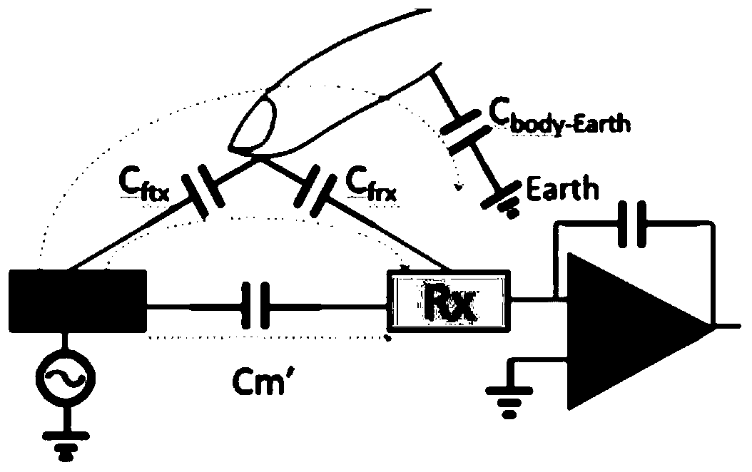
[0043] In the related art, the schematic diagram of the circuit structure of the ultra-thin stack structure in the case of weak grounding is as follows: figure 1 As shown, in the case of weak grounding, the capacitance C formed between the finger and the earth Earth body-Earth is very small, and the ability of this path to pass current is very weak, resulting in a small change in the total equivalent capacitance detected on the sensing electrode block RX; even due to the capacitance C formed between the finger and the driving electrode block TX ftx , and the capacitance C formed by the finger and the sensing electrode block RX frx The connection will lead to the increase of the total equivalent capacitance. However, the touch chip connected to the sensing electrode block RX can normally detect the touch position only when the reduction of the total equivalent capacitance is greater than the preset threshold, and the reduction of the total equivalent capacitance is small, or t...


PUM


Abstract

The invention discloses a touch substrate and a display device. The touch substrate comprises a substrate body, a touch driving electrode, a touch sensing electrode and a grounding electrode, whereinthe touch driving electrode, the touch sensing electrode and the grounding electrode are located on the substrate body and insulated from one another. The orthographic projection of the grounding electrode on the substrate base plate and the orthographic projection of the touch driving electrode and the touch sensing electrode on the substrate base plate have non-overlapping areas. A grounding electrode is arranged on a touch substrate. The capacitance formed between the fingers and the ground is increased. Therefore, the capacitance formed by the finger and the ground, the capacitance formedby the finger and the touch driving electrode and the capacitance formed by the finger and the touch sensing electrode are connected in parallel, the total equivalent capacitance is reduced, the variation of the total equivalent capacitance is increased, the detection of a touch chip on a touch point is facilitated, and the detection accuracy of the touch point is improved.

Description

technical field [0001] The present invention relates to the technical field of touch display, in particular to a touch substrate and a display device. Background technique [0002] With the development of display technology, people have higher and higher requirements for display panels, and gradually tend to ultra-thin and flexible and bendable display panels. Among them, the integrated thinning of the module stack structure is conducive to bending, curling and other requirements. [0003] However, as the thickness of the module stack structure becomes thinner, the mutual capacitive touch structure is prone to abnormal detection of touch points under the condition of low ground mass (LGM). Specifically, in the case of weak grounding, the capacitance formed between the finger and the ground is very small, and the current passing capacity of this path is very weak, resulting in a decrease in the mutual capacitance change detected by the touch chip. Capacitance, as well as the...

Claims


Application Information

Patent Timeline
Patent Type & Authority Applications(China)
IPC IPC(8): G06F3/041
CPCG06F3/0412G06F3/0448G06F2203/04111G06F2203/04107G06F3/0446G06F3/0443G06F3/04164
Inventor 薄赜文项大林
Owner BOE TECH GRP CO LTD
Why Eureka
Try Eureka