Eureka AIR delivers breakthrough ideas for toughest innovation challenges, trusted by R&D personnel around the world.

Semiconductor process method and semiconductor structure

A technology of semiconductor and process, applied in the direction of semiconductor devices, semiconductor/solid-state device manufacturing, electric solid-state devices, etc.

Active Publication Date: 2020-03-10
TAIWAN SEMICON MFG CO LTD
View PDF12 Cites 0 Cited by
  • Summary
  • Abstract
  • Description
  • Claims
  • Application Information

AI Technical Summary

Problems solved by technology

Downscaling (alone and in combination with new and different materials) also presents challenges that previous generations may not have presented in larger geometries

Method used


Image

  • Semiconductor process method and semiconductor structure
  • Semiconductor process method and semiconductor structure
  • Semiconductor process method and semiconductor structure

Examples


example 1

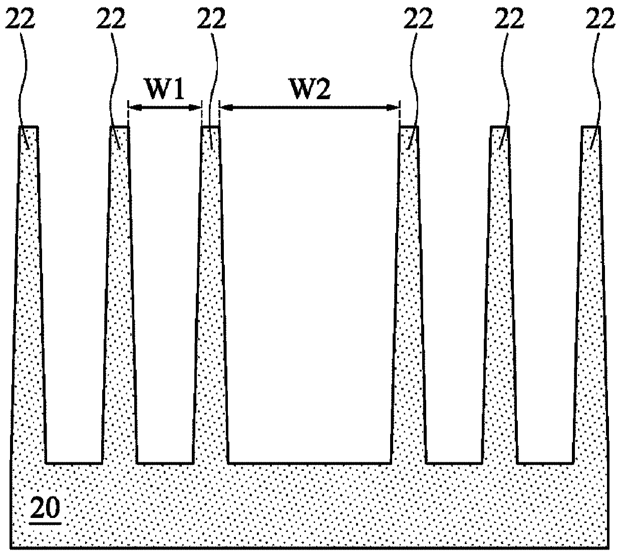
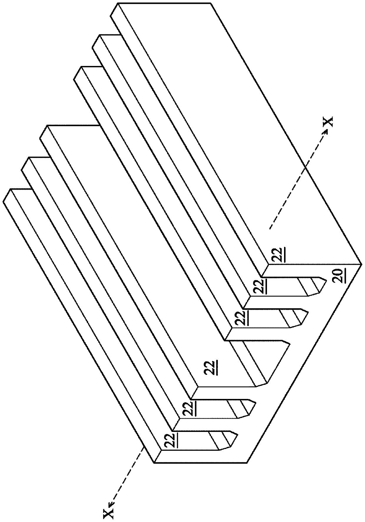
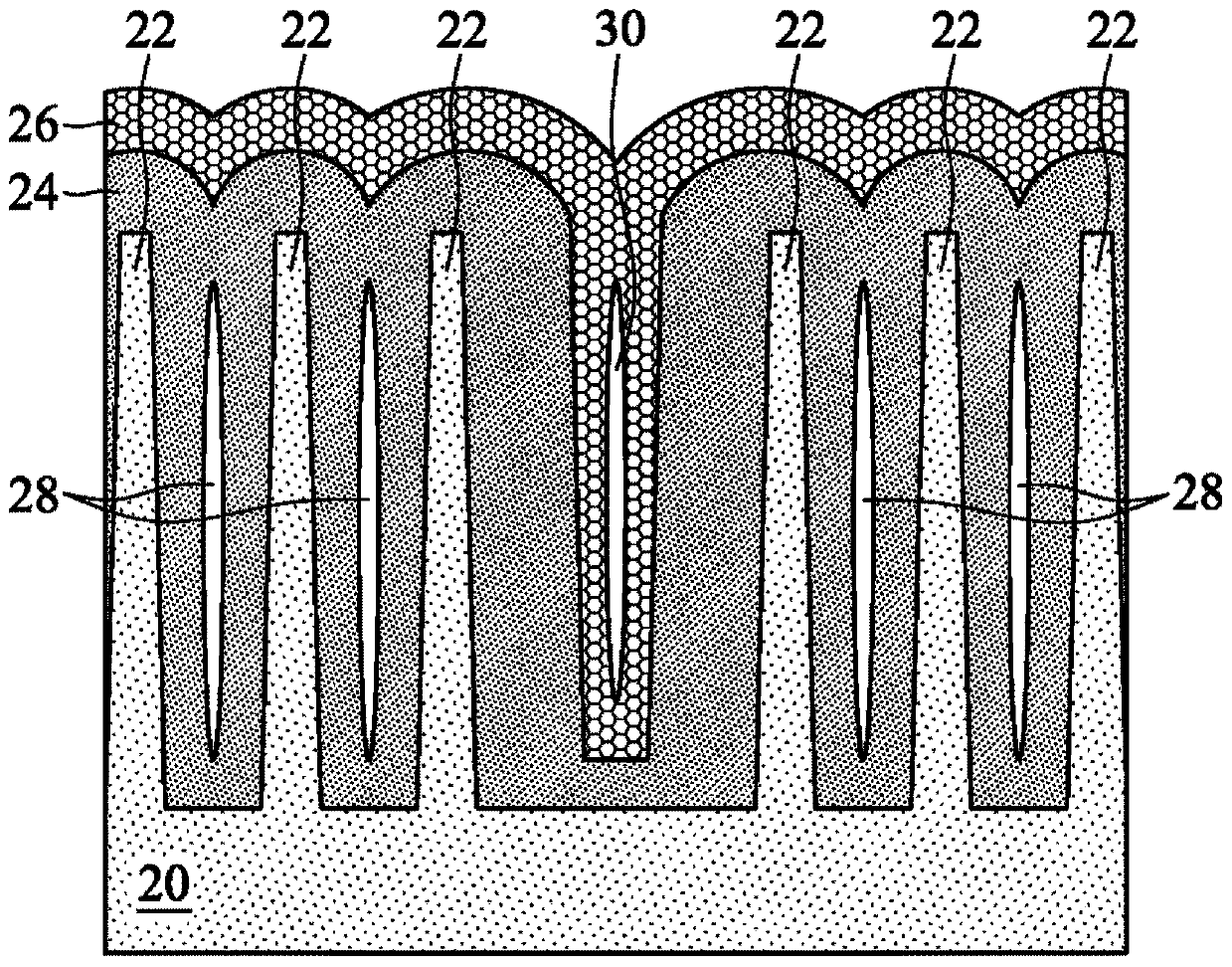
[0076] Example 1 is a method of semiconductor processing comprising conformally depositing a first dielectric material in a first trench in a substrate and in a second trench in the substrate, wherein the The merged lateral growth front of the first dielectric material in the first trench forms a seam in the first trench; treating the first dielectric material and the second trench in the first trench said first dielectric material in a trench, said first dielectric material in said first trench has a first upper surface, said first dielectric material in said second trench has a second upper surface, The treatment causes species to diffuse on the first upper surface and the second upper surface, in the seam, and into the first dielectric material in the first trench and into the in the first dielectric material in the second trench; and after the treating, etching the first dielectric material in the first trench and the first dielectric material in the second trench A diele...


PUM


Abstract

The invention relates to a semiconductor process method and a semiconductor structure. Generally, this disclosure provides examples relating to tuning etch rates of dielectric material. In an embodiment, a dielectric material is conformally deposited in first and second trenches in a substrate. Merged lateral growth fronts of the first dielectric material in the first trench form a seam in the first trench. The dielectric material is treated. The treating causes a species to be on first and second upper surfaces of the dielectric material in the first and second trenches, respectively, to be in the seam, and to diffuse into the respective dielectric material in the first and second trenches. After the treating, the respective dielectric material is etched. A ratio of an etch rate of the dielectric material in the second trench to an etch rate of the dielectric material in the first trench is altered by presence of the species in the dielectric material during the etching.

Description

technical field [0001] The present disclosure relates to methods of semiconductor processing and semiconductor structures. Background technique [0002] The semiconductor integrated circuit (IC) industry has experienced exponential growth. Technological advances in IC materials and design have produced several generations of ICs, each of which has smaller and more complex circuits than the previous generation. In the course of IC evolution, functional density (eg, the number of interconnected devices per chip area) typically increases, while geometry size (eg, the smallest component (or line) that can be produced using a fabrication process) decreases. This downscaling process often provides benefits by increasing production efficiency and reducing associated costs. [0003] As devices shrink, manufacturers have begun using new and different materials and / or combinations of materials to facilitate device shrinking. Downscaling (alone and in combination with new and differ...

Claims


Application Information

Patent Timeline
Patent Type & Authority Applications(China)
IPC IPC(8): H01L21/8234
CPCH01L21/823431H01L21/823481H01L29/66545H01L29/6681H01L27/0886H01L21/31116H01L21/76224H01L21/0228H01L21/02126H01L21/764H01L21/76229H01L29/66795H01L21/31105H01L21/76837H01L21/823468H01L21/31051H01L21/31144H01L29/0649H01L21/02271
Inventor 陈世强李俊鸿陈嘉仁林泓纬毛隆凯
Owner TAIWAN SEMICON MFG CO LTD
Why Eureka
Eureka Blog
Learn More