
Display driving board, preparation method thereof and display device

A technology for displaying driver boards and display areas, applied in static indicators, instruments, electrical components, etc., and can solve the problems of poor side routing, thin thickness, and excessive resistance.

Active Publication Date: 2020-03-24
BOE TECH GRP CO LTD +1
View PDF6 Cites 6 Cited by
  • Summary
  • Abstract
  • Description
  • Claims
  • Application Information

AI Technical Summary

Problems solved by technology

It is used to solve the problems of excessive resistance when the side traces contact the first pad and poor pad printing of the side traces caused by factors such as thin thickness of the first pad, edge chipping, and protective glue wrapping in the related art.

Method used


Image

  • Display driving board, preparation method thereof and display device
  • Display driving board, preparation method thereof and display device
  • Display driving board, preparation method thereof and display device

Examples


Embodiment Construction

[0032] The following will clearly and completely describe the technical solutions in the embodiments of the present invention with reference to the accompanying drawings in the embodiments of the present invention. Obviously, the described embodiments are only some, not all, embodiments of the present invention. Based on the embodiments of the present invention, all other embodiments obtained by persons of ordinary skill in the art without making creative efforts belong to the protection scope of the present invention.

[0033] In describing the present invention, it is to be understood that the terms "center", "upper", "lower", "front", "rear", "left", "right", "vertical", "horizontal", The orientations or positional relationships indicated by "top", "bottom", "inner", "outer", etc. are based on the orientations or positional relationships shown in the drawings, and are only for the convenience of describing the present invention and simplifying the description, rather than in...


PUM

PropertyMeasurementUnit
Thicknessaaaaaaaaaa
Hardnessaaaaaaaaaa

Abstract

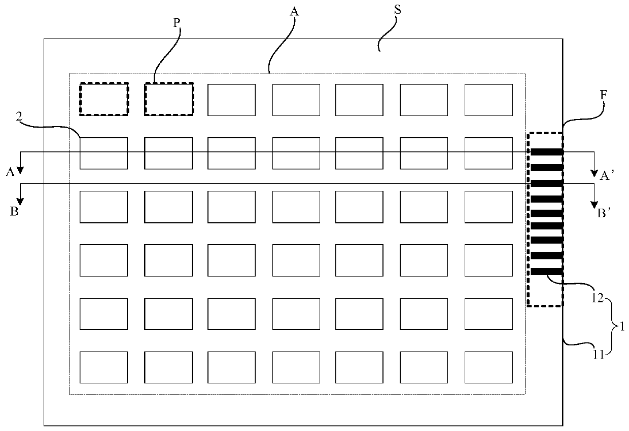
The invention relates to the technical field of display, in particular to a display driving board, a preparation method thereof and a display device. The problems that in the prior art, due to the facts that the thickness of a first bonding pad is small, edge breakage occurs, and protection glue wraps the first bonding pad, resistance is too large when side face wiring makes contact with the firstbonding pad, and side face wiring pad printing is poor are solved. In the display driving board provided by the embodiment of the invention, the display driving board is provided with a display areaand a peripheral area, and the peripheral area comprises a binding area close to the first side of the display driving board; the display driving board comprises a substrate layer and a plurality of spaced first bonding pads which are arranged on the substrate layer and located in the binding area. One side face of each first bonding pad is flush with the first side face of the substrate layer, and the first side face of the substrate layer is the side face, corresponding to the first side of the display driving board, of the substrate layer. And the thickness of the first bonding pad is 0.5-2microns. The embodiment of the invention is used for increasing the contact area of the side wiring and the first bonding pad.

Description

technical field [0001] The invention relates to the field of display technology, in particular to a display driving board, a preparation method thereof, and a display device. Background technique [0002] The size of the light-emitting diodes used in the light-emitting diode display device is on the micron level, and it has the characteristics of independent control of the picture, independent light-emitting control, high brightness, low power consumption, ultra-high resolution and high color saturation. It will become one of the hot spots in the development of display technology in the future. Contents of the invention [0003] The main purpose of the present invention is to provide a display driving board, a manufacturing method thereof, and a display device. It is used to solve the problems of excessive resistance when the side traces are in contact with the first pad and poor printing of the side traces caused by factors such as thin thickness of the first pad, edge c...

Claims


Application Information

Patent Timeline
IPC IPC(8): H01L25/16G09G3/32
CPCH01L25/167G09G3/32G09G2300/0404H01L25/0753H01L27/124H01L33/62
Inventor 孟柯刘超崔强伟汪楚航王莉莉龚林辉初宇天杨帆
Owner BOE TECH GRP CO LTD
Learn More