A kind of multi-layer coupling structure multi-band graphene detector and preparation process thereof

A technology of coupling structure and preparation process, which is applied in the field of multi-layer coupling structure multi-band graphene detector and its preparation process, can solve the problems of low responsivity, low quantum effect, and inability to detect multi-band high-response, so as to improve the response degree, photoelectric response enhancement, and the effect of improving carrier transport efficiency

Active Publication Date: 2021-07-13
XI AN JIAOTONG UNIV
View PDF0 Cites 0 Cited by
  • Summary
  • Abstract
  • Description
  • Claims
  • Application Information

AI Technical Summary

Problems solved by technology

[0003] The purpose of the present invention is to provide a multi-layer coupling structure multi-band graphene detector and its preparation process to solve the problems of low responsivity, low quantum effect and incapable of multi-band high-response detection of existing graphene photodetectors

Method used


Image

  • A kind of multi-layer coupling structure multi-band graphene detector and preparation process thereof

Examples


Embodiment

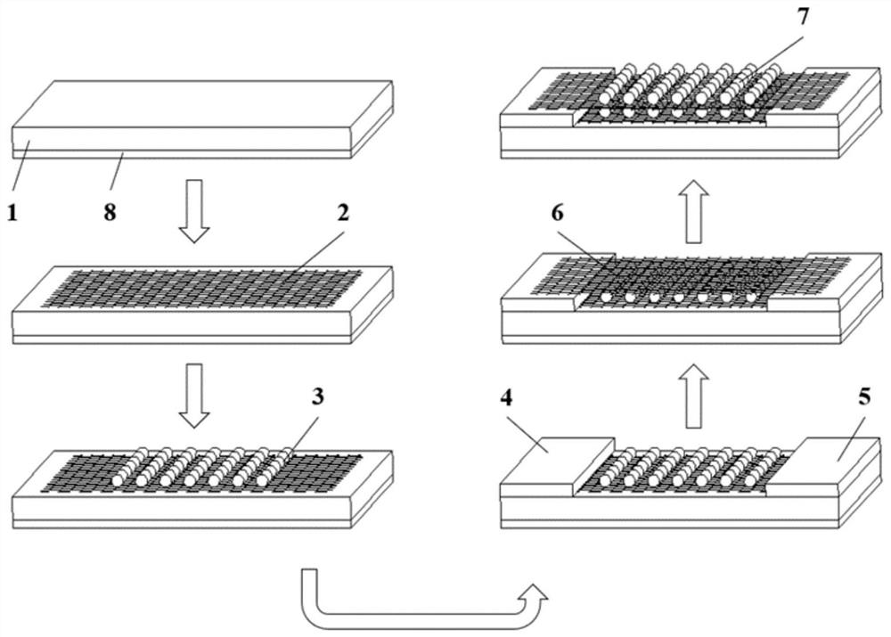
[0036] In order to realize the multi-band graphene detector with multi-layer coupling structure, the present invention provides a reliable and efficient preparation process. Such as figure 1 shown, including the following steps:

[0037] 1) Electron beam evaporation on the silicon side of the silicon dioxide / silicon substrate to prepare a 100nm thick Au back gate;

[0038] 2) Graphene is grown by chemical vapor deposition and transferred to a silicon dioxide / silicon substrate;

[0039] 3) Utilize electron beam evaporation to deposit one deck of 15nm thick metal nano film on the graphene of step 2);

[0040] 4) Annealing the sample deposited with the metal nano film at 500° C. for 90 min in a nitrogen atmosphere to obtain bottom metal nanoparticles;

[0041] 5) Prepare metal electrodes at both ends of the graphene;

[0042] 6) transfer a layer of graphene grown by chemical vapor deposition on the metal electrode;

[0043] 7) Utilize electron beam evaporation to deposit one...


PUM

PropertyMeasurementUnit
thicknessaaaaaaaaaa

Abstract

The invention discloses a multi-layer coupling structure multi-band graphene detector and a preparation process thereof. The detector consists of a silicon dioxide / silicon substrate, bottom graphene, bottom metal nanoparticles, source, drain, top graphene, top metal nanoparticles and a back gate. A sandwich structure of metal electrodes between two layers of graphene, forming a double active layer. Two layers of metal nanoparticles modify the structure of two layers of graphene to achieve enhanced photoelectric response to dual-band and multi-band. By controlling the two layers of metal nanoparticles separately, changing the size, material and particle distance of the metal nanoparticles, the selective absorption enhancement of incident light of a specific wavelength and the selective photodetection of multiple bands are realized. The regulation of the back gate voltage further enhances the light absorption and improves the responsivity. The detector has a simple preparation process, realizes high-speed, high-sensitivity, and multi-band detection at room temperature, and effectively solves the urgent needs of dual-band and multi-band detection.

Description

technical field [0001] The invention belongs to the fields of material science, semiconductor optoelectronic devices and micro-nano manufacturing, and specifically relates to a multi-layer coupling structure multi-band graphene detector and a preparation process thereof. Background technique [0002] Photodetectors are not only widely used in various fields of military, national defense and national economy, but also have penetrated into many disciplines and developed rapidly. Such as: night vision reconnaissance, weapon sights, detection of material defects, thermal diagnosis of equipment status, production process monitoring, disaster reduction and prevention, and many other aspects. As an emerging two-dimensional material, graphene can be used in the field of photodetection to detect the entire spectrum from ultraviolet to visible light to infrared. Graphene photodetectors overcome the shortcomings of third-generation detectors such as mercury cadmium telluride (HgCdTe) ...

Claims


Application Information

Patent Timeline
Patent Type & Authority Patents(China)
IPC IPC(8): H01L31/113H01L31/0216H01L31/18
CPCH01L31/02161H01L31/1136H01L31/1804Y02P70/50
Inventor 杨树明索浩王一鸣吉培瑞
Owner XI AN JIAOTONG UNIV
Why Eureka
Try Eureka