Photomask assembly and lithography method

A component and photomask technology, which is applied to the original parts for photomechanical processing, optics, photomechanical equipment, etc., can solve the problem of inability to accurately form through holes or island structures with high aspect ratios, difficult exposure of the bottom of the photoresist, etc. Problems such as photoresist overexposure

Active Publication Date: 2020-04-03
SHANGHAI HUALI MICROELECTRONICS CORP
View PDF6 Cites 0 Cited by
  • Summary
  • Abstract
  • Description
  • Claims
  • Application Information

AI Technical Summary

Problems solved by technology

[0004] The object of the present invention is to provide a photomask assembly and a photolithography method to solve the problem that the existing photomask assembly and photolithography method easily lead to overexposure of the top of the photoresist, and make the bottom of the photoresist difficult to be exposed, so that it cannot be accurately exposed. Problems forming high aspect ratio vias or island structures

Method used


Image

  • Photomask assembly and lithography method
  • Photomask assembly and lithography method
  • Photomask assembly and lithography method

Examples


Embodiment Construction

[0030] The photomask assembly and photolithography method proposed by the present invention will be further described in detail below with reference to the accompanying drawings and specific embodiments. The advantages and features of the present invention will be more apparent from the following description. It should be noted that all the drawings are in a very simplified form and use imprecise scales, and are only used to facilitate and clearly assist the purpose of illustrating the embodiments of the present invention.

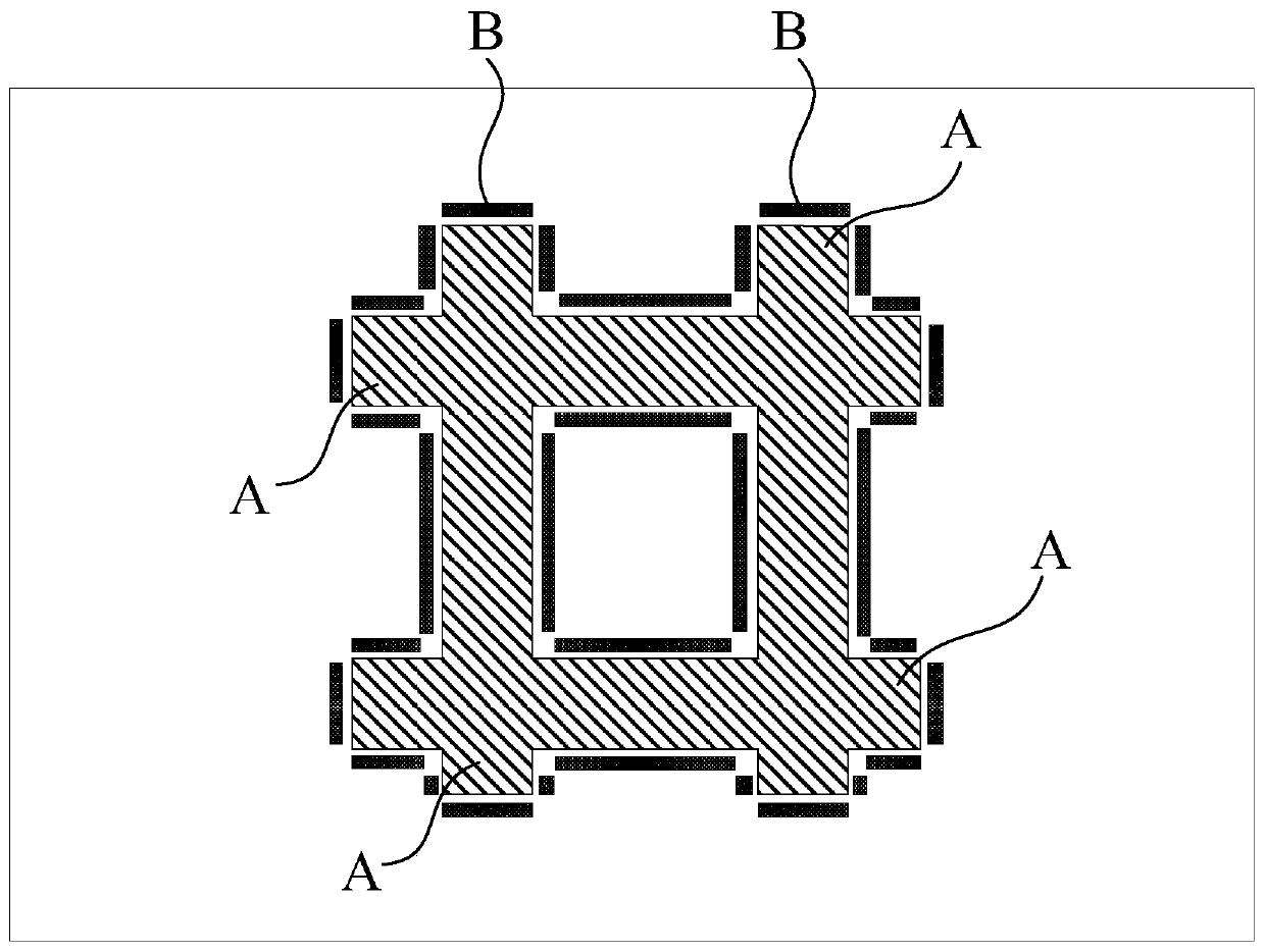
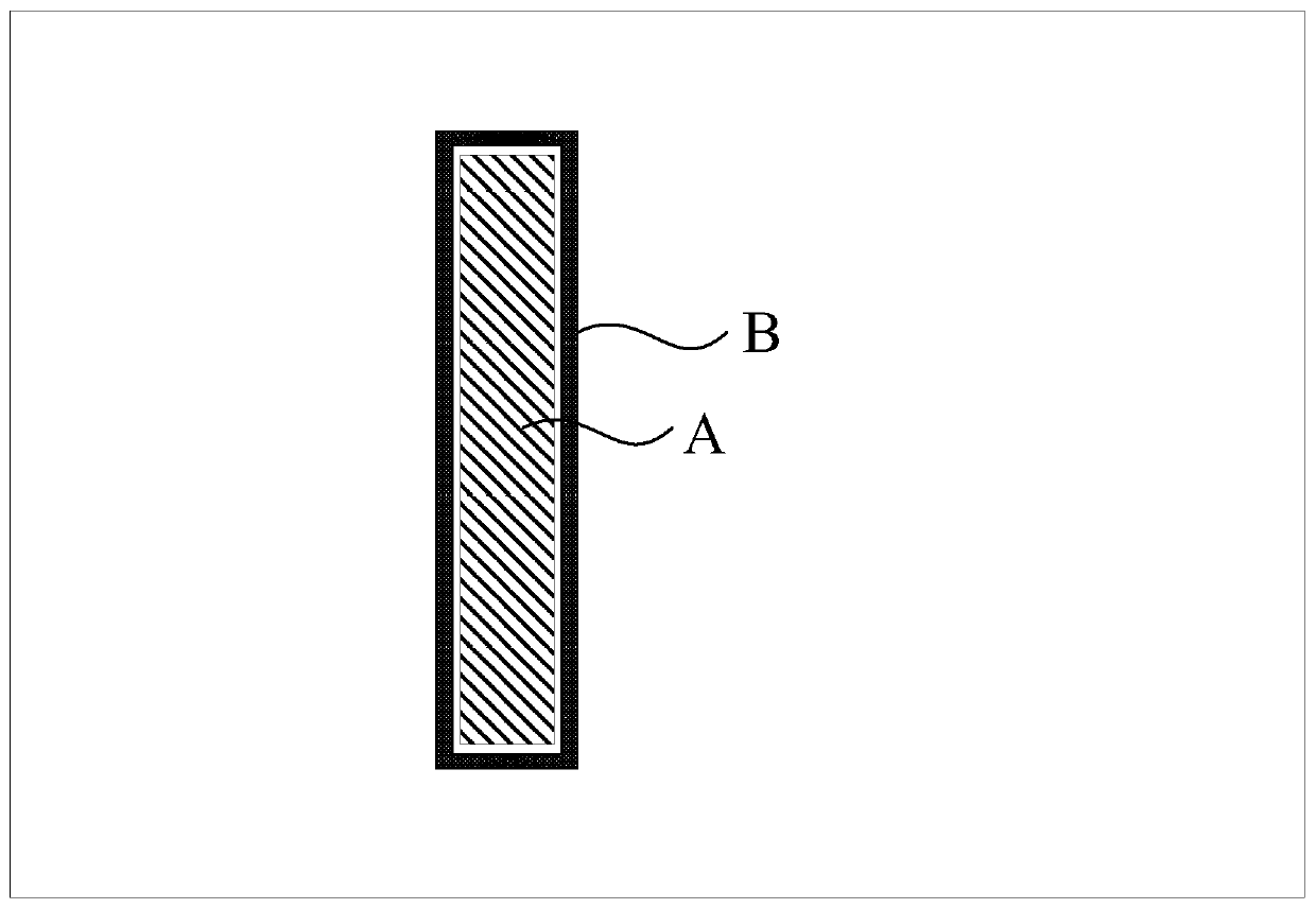
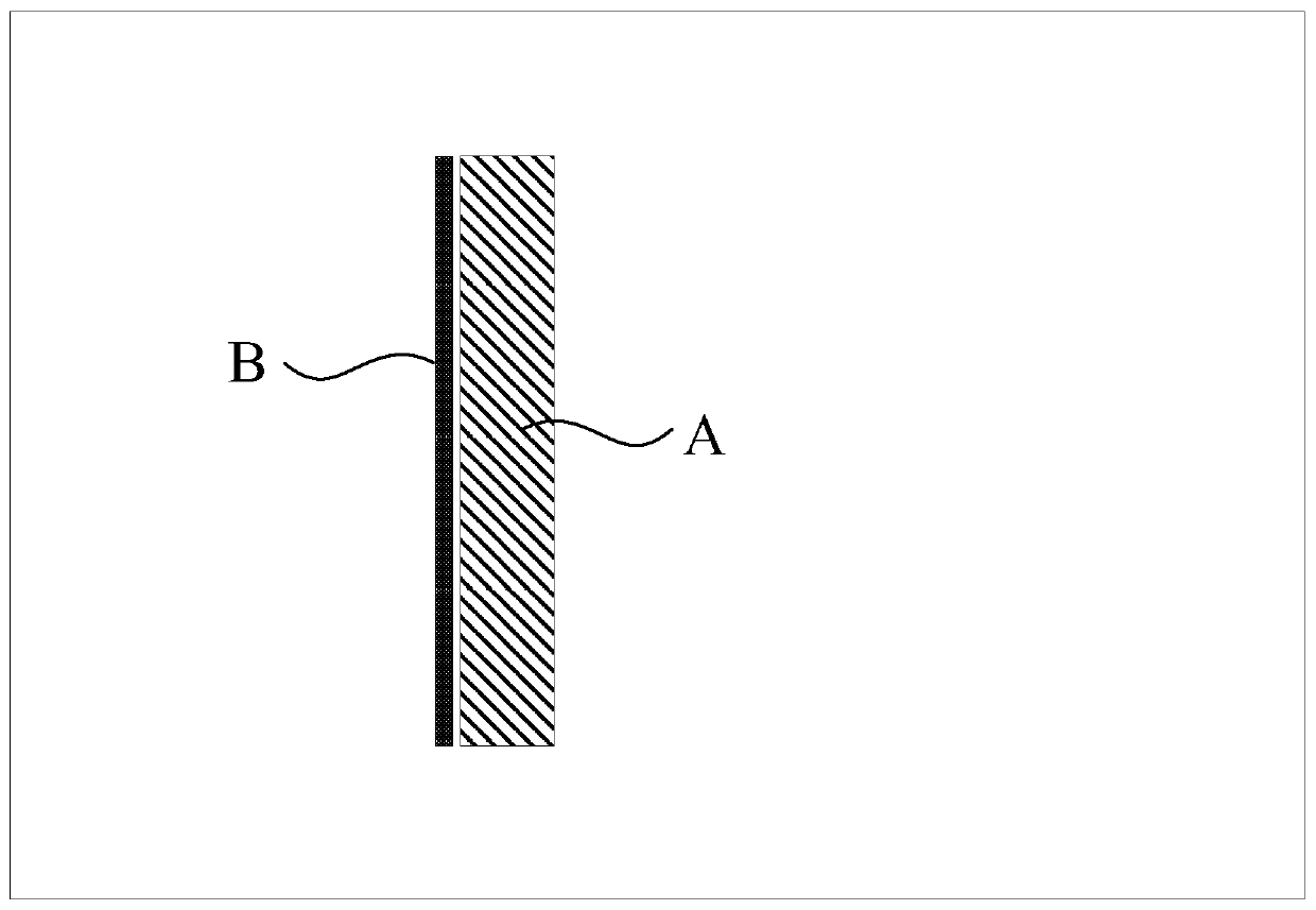
[0031] figure 1 A schematic structural diagram of a photomask assembly provided by an embodiment of the present invention, such as figure 1 Said, the mask assembly may include at least one target pattern A and at least one auxiliary pattern B.

[0032] Wherein, the auxiliary pattern B is arranged adjacent to the target pattern A, and the target pattern A can define the target light-transmitting area of ​​the mask assembly (for example, the light shaded p...


PUM


Abstract

The invention provides a photomask assembly and a photoetching method, and the photomask assembly comprises: at least one target pattern, wherein the target pattern defines the target light transmission region of the photomask assembly, and the pattern of the at least one target pattern is used for being copied to a photoresist layer; and at least one auxiliary pattern which is arranged adjacent to the at least one target pattern, defines the auxiliary light-transmitting area of the photomask assembly, and is used for enabling a light beam to pass through the auxiliary light-transmitting areato irradiate into the photoresist layer corresponding to the target light-transmitting area during exposure. When the photomask assembly is used for executing the photoetching method, a through hole or island-shaped structure with a high depth-to-width ratio can be accurately formed in the substrate.

Description

technical field [0001] The invention relates to the technical field of semiconductor manufacturing, in particular to a photomask assembly and a photolithography method. Background technique [0002] In the field of semiconductors, in order to form via holes or island structures with high aspect ratios, a thicker photoresist layer is usually coated on the surface of the substrate during the photolithography process, and a photomask is used to coat the photoresist layer. The second exposure is performed to copy the pattern on the photomask to the photoresist layer, and then the development step is performed to form openings or island-like structures in the photoresist layer. After that, the previously formed photoresist structure Based on ion implantation. [0003] However, in the related art, when performing secondary exposure on the photoresist layer, since the thickness of the photoresist layer is relatively thick, the energy of the light beam is usually increased to incre...

Claims


Application Information

Patent Timeline
Patent Type & Authority Applications(China)
IPC IPC(8): G03F1/38G03F7/00
CPCG03F1/38G03F7/0035
Inventor 王传龙赵彬王剑
Owner SHANGHAI HUALI MICROELECTRONICS CORP
Why Eureka
Try Eureka