A Tightly Coupled Miniaturized Metamaterial Structure

A metamaterial and tightly coupled technology, applied in the microwave field, can solve the problems of limited miniaturization, complex process, large distributed capacitance, etc., and achieve the effect of miniaturization, simple process, and reduction of the overall size of the structure

Active Publication Date: 2021-08-06
武汉灵动时代智能技术股份有限公司
View PDF5 Cites 0 Cited by
  • Summary
  • Abstract
  • Description
  • Claims
  • Application Information

AI Technical Summary

Problems solved by technology

This method exists: 1. The degree of miniaturization is limited (because the smallest lumped device specification is 0201, the length is 0.6mm, and the width is 0.3mm, so the gap size of the distributed capacitor cannot be less than 0.5mm, but the actual PCB processing technology can be Make the gap 0.05mm, the smaller the gap between the equivalent capacitance structures, the larger the distributed capacitance); 2. The process is complex; 3. The higher the degree of miniaturization, the larger the loaded lumped capacitance, resulting in grating lobes also bigger

Method used


Image

  • A Tightly Coupled Miniaturized Metamaterial Structure
  • A Tightly Coupled Miniaturized Metamaterial Structure
  • A Tightly Coupled Miniaturized Metamaterial Structure

Examples


Embodiment Construction

[0019] The specific implementation manners of the present invention will be further described in detail below in conjunction with the accompanying drawings and embodiments. The following examples are used to illustrate the present invention, but are not intended to limit the scope of the present invention.

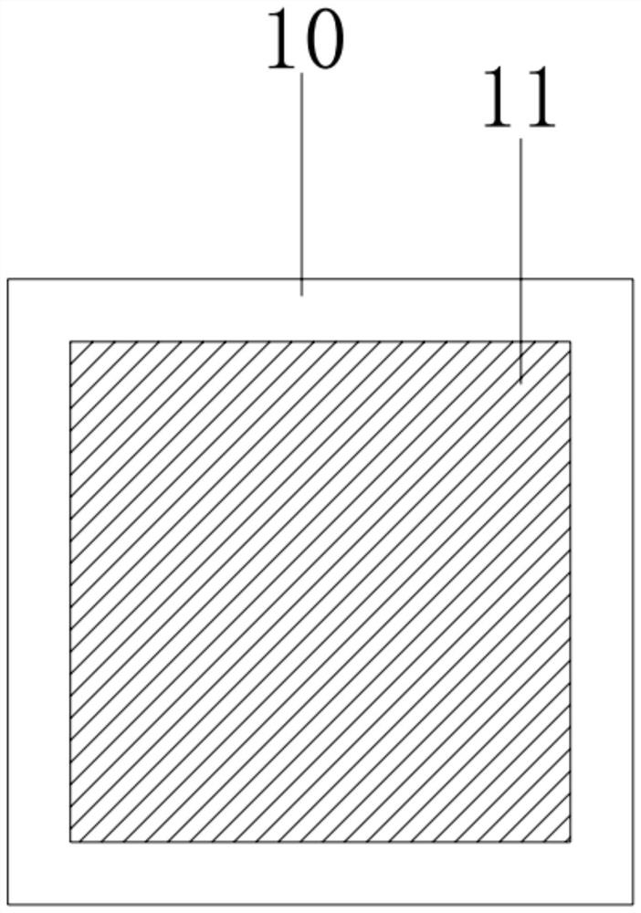
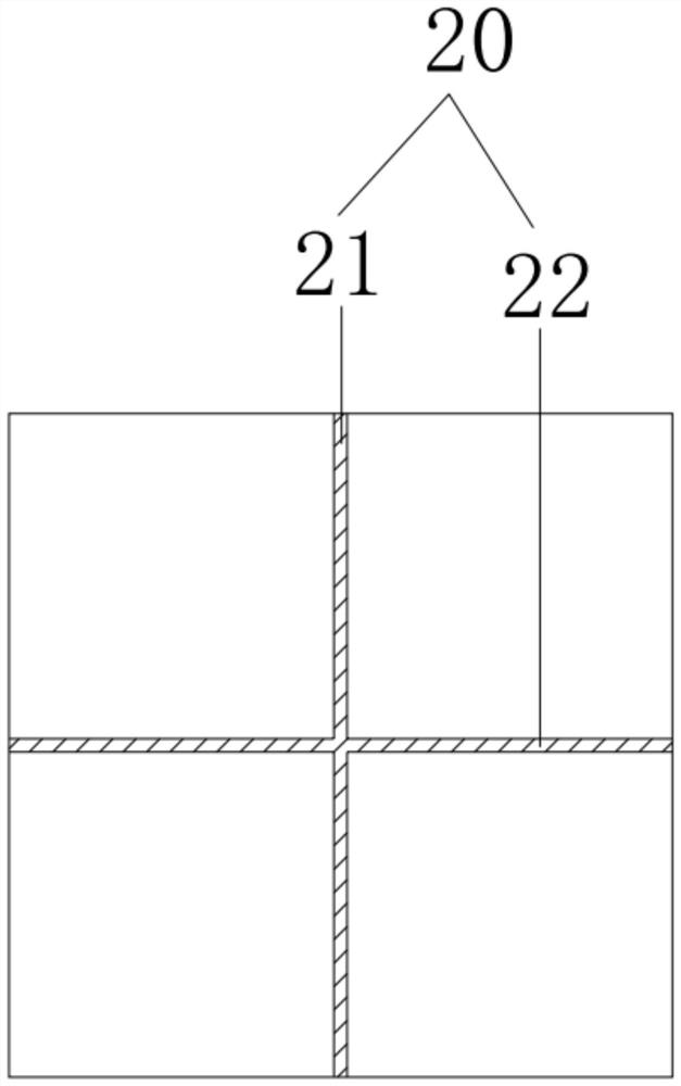
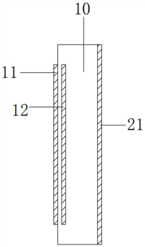
[0020] see figure 1 , and combined with figure 2 and image 3 As shown, a tightly coupled miniaturized metamaterial structure of the present invention includes a dielectric substrate 10, wherein a printed metal layer 11 is provided on one end surface of the dielectric substrate 10, and a cross-shaped metal layer 11 is provided on the other end surface of the dielectric substrate 10. Shaped metal frame 20 , and a coupling capacitor layer 12 is embedded in the dielectric substrate 10 .

[0021] Wherein, the area of ​​the printed metal layer 11 is smaller than the area of ​​the dielectric substrate 10, and the coupling capacitance layer 12 is arranged on the side of the d...


PUM


Abstract

A tightly coupled miniaturized metamaterial structure of the present invention includes a dielectric substrate, a printed metal layer is provided on one end surface of the dielectric substrate, and a cross-shaped metal frame is provided on the other end surface of the dielectric substrate. There is also a coupling capacitor layer embedded in it. A tightly coupled miniaturized metamaterial structure of the present invention forms an inductance structure by using a cross-shaped metal frame, and utilizes the interaction between the embedded coupling capacitor layer and the printed metal layer in the dielectric substrate to form a parallel capacitor structure , resulting in a larger equivalent capacitance, thereby reducing the size of the metamaterial structure and realizing the miniaturization of the metamaterial.

Description

technical field [0001] The invention relates to the field of microwaves, and more specifically, relates to a tightly coupled miniaturized metamaterial structure. Background technique [0002] The wide coverage of radar and various wireless devices has resulted in a tight use of spectrum resources. Multi-frequency communication and multi-frequency radar have become the direction of rapid development in the modern microwave field, followed by mutual interference between devices in different frequency bands. Because the metamaterial structure can frequency-select and filter electromagnetic waves in space and shield out-of-band signals, the study of metamaterial structures is of great significance. [0003] The metamaterial structure can filter electromagnetic waves in space, and exhibits obvious band-pass or band-resistance characteristics when interacting with electromagnetic waves. It is a two-dimensional periodic array structure composed of periodically arranged metal patche...

Claims


Application Information

Patent Timeline
Patent Type & Authority Patents(China)
IPC IPC(8): H01Q15/00
CPCH01Q15/0026
Inventor 张岭陈志勇
Owner 武汉灵动时代智能技术股份有限公司
Why Eureka
Try Eureka