Dust removal device for PCB

A technology of PCB board and dust removal device, which is applied in the field of PCB board manufacturing, can solve the problems that it is not suitable for large-scale cleaning, not suitable for small and medium-sized enterprises, and low cleaning efficiency, and achieves the effects of cost reduction, fast installation and disassembly, and high dust removal efficiency.

Inactive Publication Date: 2020-04-07
ANHUI TIANBING ELECTRONICS TECH
View PDF9 Cites 5 Cited by
  • Summary
  • Abstract
  • Description
  • Claims
  • Application Information

AI Technical Summary

Problems solved by technology

[0002] The PCB board needs to be dedusted during the manufacturing process to prevent the presence of dust on the PCB board and affect the component welding and circuit direction. Currently, the cleaning of the PCB board is usually done manually, but t

Method used


Image

  • Dust removal device for PCB
  • Dust removal device for PCB
  • Dust removal device for PCB

Examples


Embodiment Construction

[0017] In order to make the technical means, creative features, goals and effects achieved by the present invention easy to understand, the present invention will be further described below in conjunction with specific embodiments.

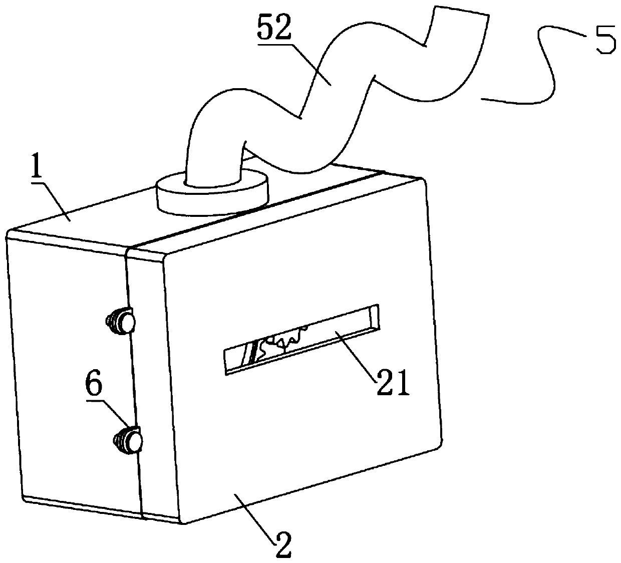
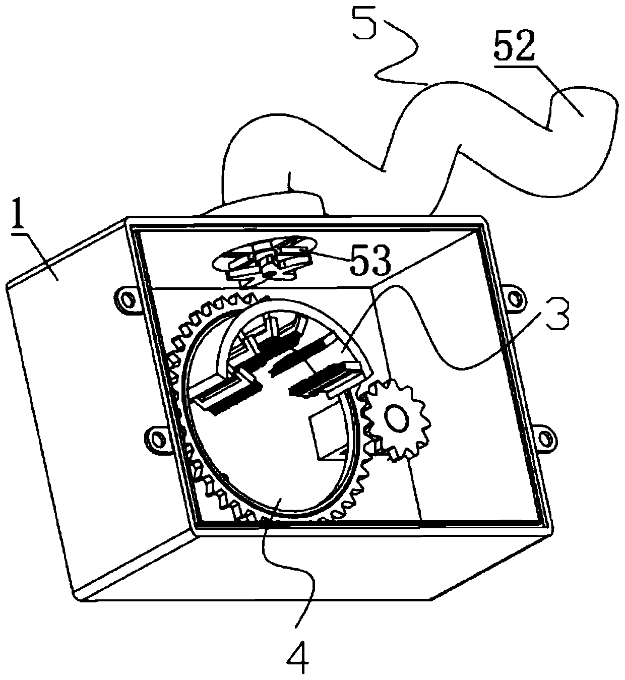
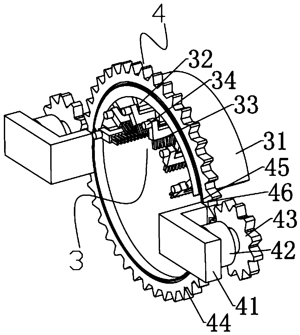
[0018] Such as Figure 1 to Figure 5 As shown, a dust removal device for a PCB board includes a rear case 1, a front case 2, a dust removal mechanism 3, a driving mechanism 4, and a dust suction mechanism 5. The rear case 1 is screwed to the front case 2, and the There is a feed port 21 on the front of the front housing 2, the dust removal mechanism 3 is rotatably connected in the rear housing 1, the driving mechanism 4 drives the dust removal mechanism 3 to rotate around the PCB board, and the dust suction mechanism 5 is located in the rear housing Body 1 top.

[0019] In this embodiment, the drive mechanism 4 includes two symmetrically structured bases 41 installed on the inner wall of the rear housing 1, and a motor one 42 is installed on the ...


PUM


Abstract

The invention discloses a dust removal device for a PCB, which relates to the technical field of PCB manufacturing. The device comprises a rear shell, a front shell, a dust removal mechanism, a driving mechanism and a dust collection mechanism, wherein the rear shell is connected with the front shell through screws; a feeding hole is formed in the front surface of the front shell; the dust removalmechanism is rotationally connected into the rear shell; the driving mechanism drives the dust removal mechanism to rotate; and the dust collection mechanism is arranged at the top end of the rear shell. The dust removal mechanism is arranged to clean the PCB, the driving mechanism is arranged to drive the dust removal mechanism to rotate around the PCB, dead-corner-free cleaning of the PCB is realized, the dust collection mechanism is used for sucking away dust generated by sweeping, the step in which drying is needed when an ultrasonic cleaning device is used for cleaning and other steps are not needed, large generated cost is not needed, and the side surfaces of the rear shell and the front shell are provided with connecting pieces and are connected through screws, so that the rear shell and the front shell are accurately mounted and positioned, and are more quickly mounted and dismounted, and therefore, the dust removal efficiency is high, the cost is reduced, and the dust removaldevice is suitable for small and medium-sized enterprises.

Description

technical field [0001] The invention belongs to the technical field of PCB board manufacturing, and in particular relates to a dust removal device for a PCB board. Background technique [0002] The PCB board needs to be dedusted during the manufacturing process to prevent the presence of dust on the PCB board and affect the component welding and circuit direction. Currently, the cleaning of the PCB board is usually done manually, but the cleaning efficiency is not high, and it is not suitable for mass cleaning. However, cleaning with an ultrasonic cleaning device also requires steps such as drying, resulting in relatively large costs, and is not suitable for small and medium-sized enterprises. Contents of the invention [0003] The purpose of the present invention is to provide a dust removal device for PCB boards to solve the above-mentioned defects caused by the above-mentioned prior art. [0004] A dust removal device for a PCB board, comprising a rear shell, a front s...

Claims


Application Information

Patent Timeline
IPC IPC(8): B08B1/04B08B15/00
CPCB08B1/002B08B1/04B08B15/007
Inventor 陈在张东响马自若祁伟汪天骄
Owner ANHUI TIANBING ELECTRONICS TECH
Why Eureka
Try Eureka