A printed circuit board and electronic equipment

A technology for printed circuit boards and electronic equipment, applied in the field of control, can solve the problems of increasing the distance between the impedance line and the reference ground, the impedance is discontinuous, and cannot be wired, so as to increase the impedance of the RF line and reduce the area that cannot be wired. Avoid the effect of impedance discontinuities

Active Publication Date: 2022-02-18
LENOVO (BEIJING) LTD
View PDF8 Cites 0 Cited by
  • Summary
  • Abstract
  • Description
  • Claims
  • Application Information

AI Technical Summary

Problems solved by technology

[0002] At present, the demand for frequency bands is increasing, and the frequency range is becoming wider and wider, resulting in more and more antennas, and the RF architecture is becoming more and more complex; in addition, the number of PCB layers increases, the thickness of the entire PCB board decreases, the thickness of the dielectric layer decreases, and the impedance The line width is very wide, and the pin size of the device is also large. In order to avoid the problem of impedance discontinuity at the RF common end, it is necessary to dig through the position corresponding to the impedance line on the next layer of the wiring layer to avoid Increase the distance between the impedance line and the reference ground, but this leads to the fact that the layer where the impedance line reference ground is located and the corresponding position of the impedance line cannot be wired, and a large wiring space will be lost

Method used


Image

  • A printed circuit board and electronic equipment
  • A printed circuit board and electronic equipment
  • A printed circuit board and electronic equipment

Examples


Embodiment Construction

[0040] The following will clearly and completely describe the technical solutions in the embodiments of the application with reference to the drawings in the embodiments of the application. Apparently, the described embodiments are only some of the embodiments of the application, not all of them. Based on the embodiments in this application, all other embodiments obtained by persons of ordinary skill in the art without making creative efforts belong to the scope of protection of this application.

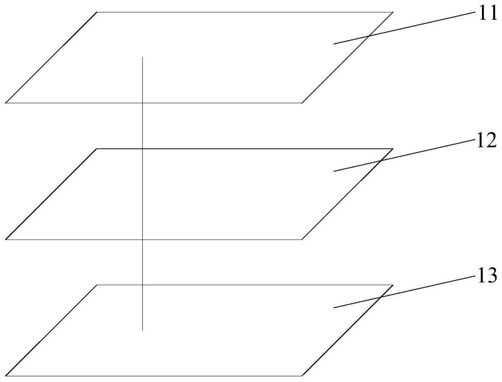
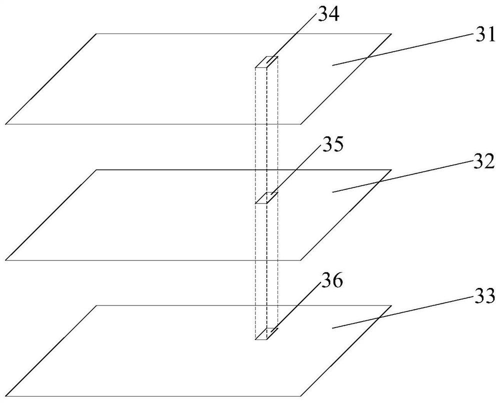
[0041] This application discloses a printed circuit board, the schematic diagram of which is as follows: figure 1 shown, including:

[0042] The top wiring layer 11, the first intermediate layer 12, and the second intermediate layer 13.

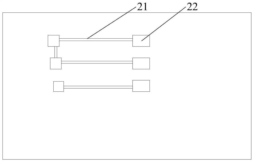
[0043] The top wiring layer 11 is provided with a plurality of radio frequency lines, and pins connected to each radio frequency line, such as figure 2 As shown, including: radio frequency line 21 and pin 22.

[0044] The first intermediate lay...


PUM


Abstract

The application discloses a printed circuit board and electronic equipment, through which the second area of ​​the second intermediate layer passes through the first area of ​​the first intermediate layer as the reference ground area of ​​the pins on the top wiring layer, so as to realize the increase of pins The distance between the pin and the reference ground of the pin is used to adjust the impedance of the radio frequency line through the increase of the distance between the pin and the reference ground of the pin, so as to avoid the problem of impedance discontinuity; The second area of ​​the first intermediate layer passes through the first area of ​​the first intermediate layer as the reference ground area of ​​the pins of the wiring layer, so that only the area corresponding to the position of the pin on the first intermediate layer cannot be wired, reducing the first intermediate layer The area that cannot be wired on the top increases the wiring space.

Description

technical field [0001] The application relates to the field of control, in particular to a printed circuit board and electronic equipment. Background technique [0002] At present, the demand for frequency bands is increasing, and the frequency range is becoming wider and wider, resulting in more and more antennas, and the RF architecture is becoming more and more complex; in addition, the number of PCB layers increases, the thickness of the entire PCB board decreases, the thickness of the dielectric layer decreases, and the impedance The line width is very wide, and the pin size of the device is also large. In order to avoid the problem of impedance discontinuity at the RF common end, it is necessary to dig through the position corresponding to the impedance line on the next layer of the wiring layer to avoid Increase the distance between the impedance line and the reference ground, however, this results in that the layer where the reference ground of the impedance line is ...

Claims


Application Information

Patent Timeline
Patent Type & Authority Patents(China)
IPC IPC(8): H05K1/02
CPCH05K1/0253
Inventor 左斌武宝东马宁
Owner LENOVO (BEIJING) LTD
Why Eureka
Try Eureka