Display panel and electronic equipment

A display panel and substrate technology, applied in static indicators, instruments, nonlinear optics, etc., can solve problems such as easy peeling of support columns and differences in output signals of GOA units, and achieve the effect of alleviating the difference in CK impedance and increasing the contact area

Active Publication Date: 2020-05-01
SHENZHEN CHINA STAR OPTOELECTRONICS SEMICON DISPLAY TECH CO LTD
View PDF5 Cites 2 Cited by
  • Summary
  • Abstract
  • Description
  • Claims
  • Application Information

AI Technical Summary

Problems solved by technology

[0006] The present application provides a display panel and electronic equipment to alleviate the technical problems of the existing 8K ultra-high resolution electronic equipment that the support columns are easy to peel off and the difference in CK impedance leads to the difference in the output signal of the GOA unit

Method used


Image

  • Display panel and electronic equipment
  • Display panel and electronic equipment
  • Display panel and electronic equipment

Examples


Embodiment Construction

[0047]The technical solutions in the embodiments of the present application will be clearly and completely described below in conjunction with the drawings in the embodiments of the present application. Apparently, the described embodiments are only some of the embodiments of this application, not all of them. Based on the embodiments in this application, all other embodiments obtained by those skilled in the art without making creative efforts belong to the scope of protection of this application.

[0048] In the description of the present application, it should be understood that the terms "center", "longitudinal", "transverse", "length", "width", "thickness", "upper", "lower", "front", " Orientation indicated by rear, left, right, vertical, horizontal, top, bottom, inside, outside, clockwise, counterclockwise, etc. The positional relationship is based on the orientation or positional relationship shown in the drawings, which is only for the convenience of describing the ap...


PUM

PropertyMeasurementUnit
thicknessaaaaaaaaaa
widthaaaaaaaaaa

Abstract

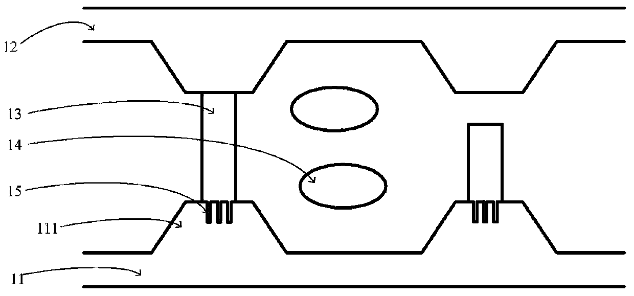
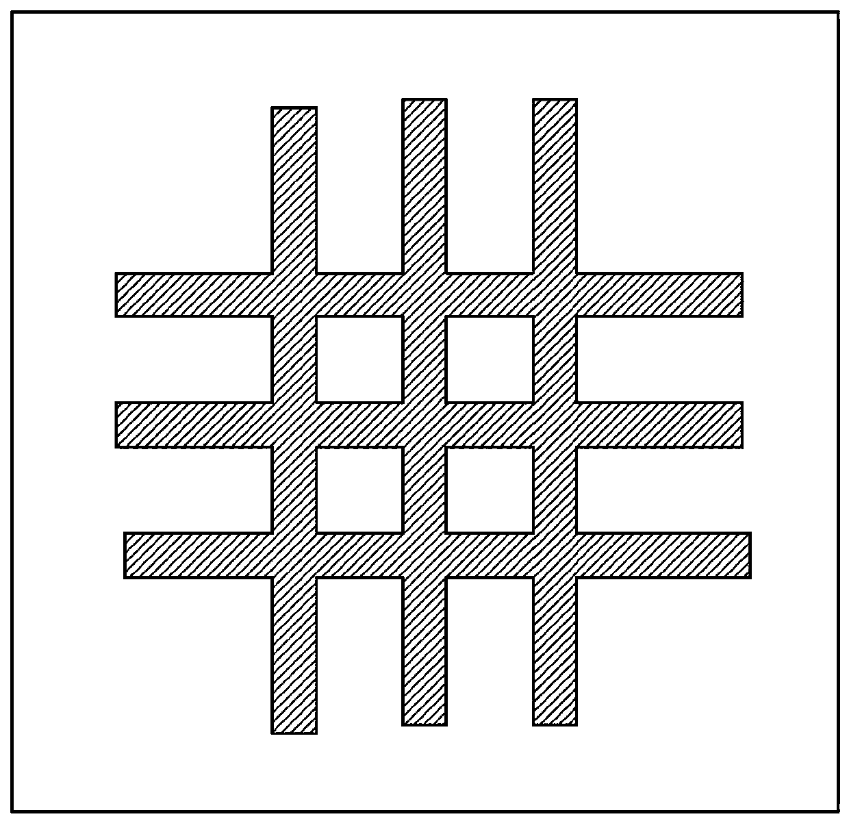
The invention provides a display panel and electronic equipment. A convex-concave pattern is formed in a contact region of a first substrate of the display panel with a supporting column, based on thestructure, contact area of the supporting column with a bottom layer is increased, and the size of a single subpixel does not need to be changed, so that the technical problem that the supporting column of existing 8K ultrahigh-resolution electronic equipment can be peeled off easily is alleviated; meanwhile, by adjusting voltage drop values of clock input transistors in different GOA units, voltage drop values between each GOA unit and a clock driving chip are approximately the same, and CK impedance difference existing in 8K ultrahigh-resolution electronic equipment is alleviated.

Description

technical field [0001] The present application relates to the field of display technology, in particular to a display panel and electronic equipment. Background technique [0002] With the development of display technology, the resolution of electronic devices such as display screens, TVs, and mobile phones is getting higher and higher. Corresponding to the increase in resolution is the increase in the number of pixels, which will bring various problems that need to be overcome. technical challenge. [0003] For example, the area of ​​a single sub-pixel of an 8K resolution electronic device is a quarter of the area of ​​a single sub-pixel of a 4K resolution electronic device, accompanied by a reduction in the contact area between the support column (ps) and the bottom layer in the panel, In an 8K resolution electronic device, the contact area between the support column and the bottom layer is 20 microns*20 microns or even smaller. Such a small contact area will cause the su...

Claims


Application Information

Patent Timeline
Patent Type & Authority Applications(China)
IPC IPC(8): G02F1/1339G02F1/1362G02F1/133G09G3/36
CPCG02F1/13394G02F1/136286G02F1/13306G09G3/3677G09G2320/0223G09G2310/0286G09G2300/0408G02F1/13454G02F1/136222G02F1/133357G02F1/136209G09G3/36G09G2310/061G09G2310/08
Inventor 廖辉华肖军城赵斌张鑫赵军
Owner SHENZHEN CHINA STAR OPTOELECTRONICS SEMICON DISPLAY TECH CO LTD
Why Eureka
Try Eureka