Dual thin film transistor and preparation method thereof, and display panel

A double-thin-film transistor and thin-film transistor technology, which is applied in transistors, semiconductor/solid-state device manufacturing, semiconductor devices, etc., can solve the problem of low mobility and achieve the effect of improving refresh efficiency

Active Publication Date: 2022-07-08
GUANGDONG JUHUA PRINTING DISPLAY TECH CO LTD
View PDF17 Cites 0 Cited by
  • Summary
  • Abstract
  • Description
  • Claims
  • Application Information

AI Technical Summary

Problems solved by technology

[0003] Based on this, it is necessary to address the technical problem of low mobility of traditional thin film transistors, to provide a double thin film transistor and its preparation method, display panel

Method used


Image

  • Dual thin film transistor and preparation method thereof, and display panel
  • Dual thin film transistor and preparation method thereof, and display panel
  • Dual thin film transistor and preparation method thereof, and display panel

Examples


Embodiment Construction

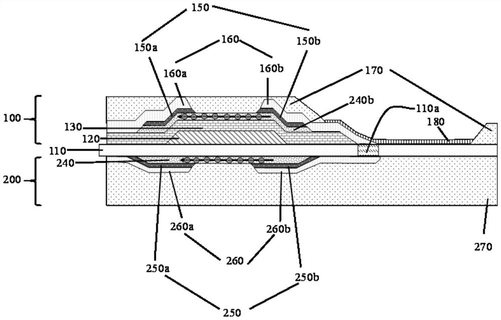
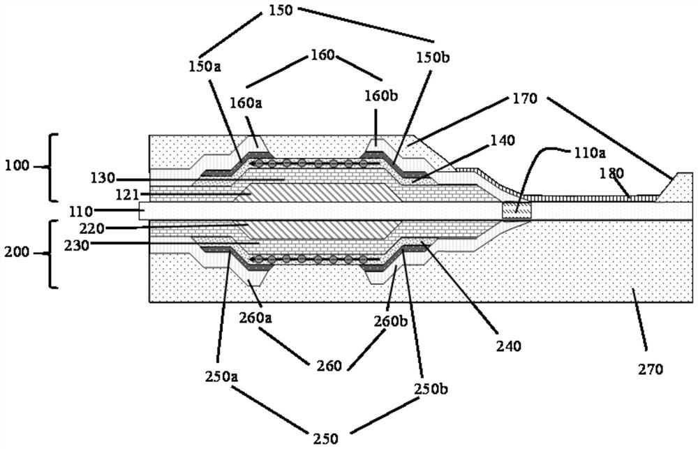
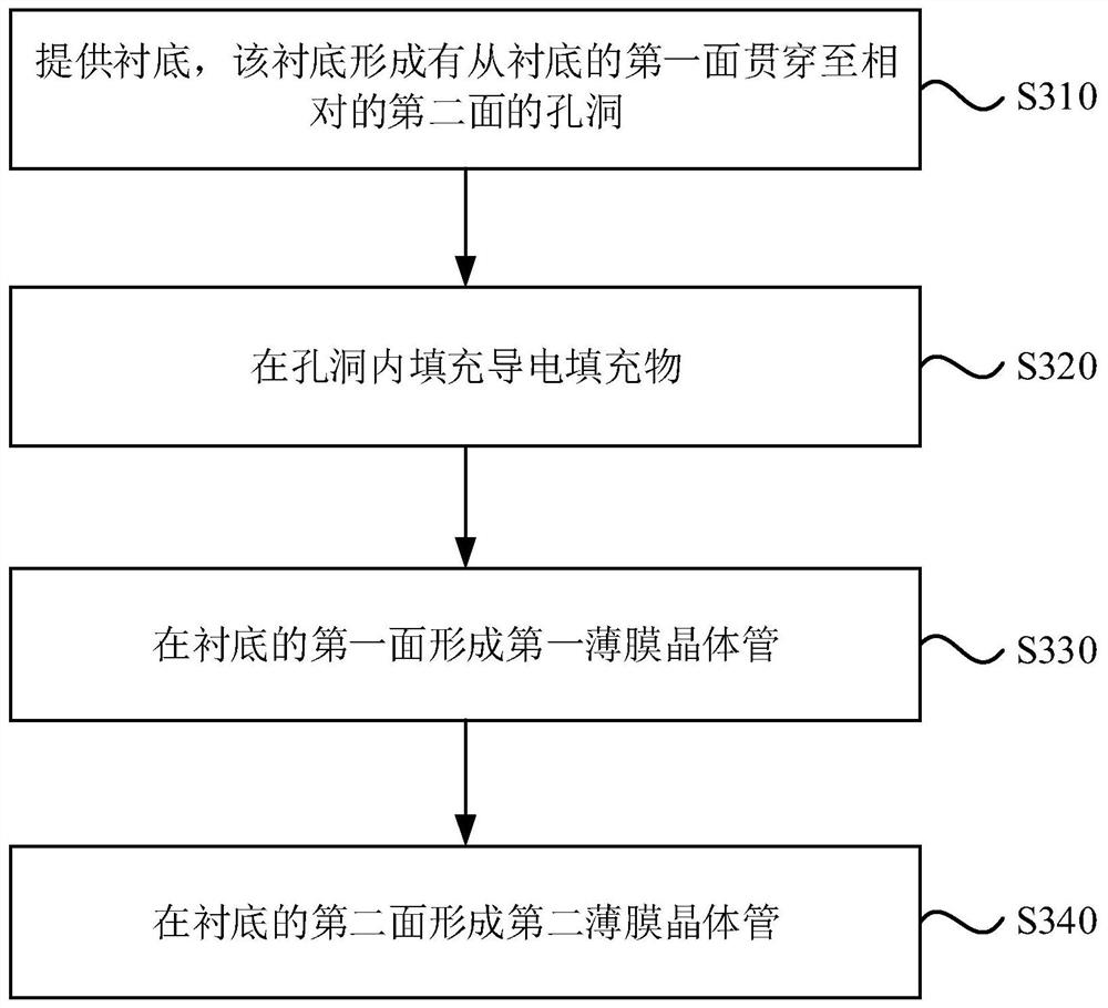
[0052] In order to facilitate understanding of the present invention, the present invention will be described more fully below. However, the present invention may be embodied in many different forms and is not limited to the embodiments described herein. Rather, these embodiments are provided so that a thorough and complete understanding of the present disclosure is provided.

[0053] Unless otherwise defined, all technical and scientific terms used herein have the same meaning as commonly understood by one of ordinary skill in the art to which this invention belongs. The terms used herein in the description of the present invention are for the purpose of describing specific embodiments only, and are not intended to limit the present invention.

[0054] It should be noted that the vacuum process in the embodiment of the present invention belongs to the prior art, which includes but is not limited to process methods such as magnetron sputtering, vacuum thermal evaporation, and...


PUM

PropertyMeasurementUnit
thicknessaaaaaaaaaa

Abstract

Embodiments of the present invention relate to a double thin film transistor, a method for fabricating the same, and a display panel. The double thin film transistor includes a first thin film transistor, a second thin film transistor, and a substrate; The first thin film transistor is located on the first surface of the substrate; the second thin film transistor is located on the second surface of the substrate; the drain of the first thin film transistor is electrically connected to the drain of the second thin film transistor through the hole The connection is so that the potentials are equal, so as to realize the double output of the leakage current and improve the refresh efficiency of the display panel.

Description

technical field [0001] The invention relates to the field of semiconductor devices, in particular to a double thin film transistor, a preparation method thereof, and a display panel. Background technique [0002] In the current flat panel display, thin film transistors are widely used as the basis of active drive display in order to achieve high resolution, so as to obtain high-speed image conversion and higher-resolution display effects. Among them, thin film transistors are an important part of active driving, and the current mainstream driving devices are amorphous silicon, polysilicon and oxide thin film transistors. Among them, as a mature driving manufacturing technology, amorphous silicon thin film transistor (TFT) device has the characteristics of low cost, less process and high yield, which makes this driving scheme widely used in low resolution high-rate TV panels as well as low-end flat-panel displays. For most high-end mobile phones on the market, Active-Matrix...

Claims


Application Information

Patent Timeline
Patent Type & Authority Patents(China)
IPC IPC(8): H01L27/088H01L21/8234H01L27/12
CPCH01L27/088H01L21/823475H01L27/124
Inventor 李松举付东唐卫东
Owner GUANGDONG JUHUA PRINTING DISPLAY TECH CO LTD
Why Eureka
Try Eureka