Resonant cavity structure and semiconductor processing equipment

A resonant cavity, resonant cavity technology, applied in discharge tubes, electrical components, circuits, etc., can solve problems such as the inability to effectively ensure the effective sealing of the elastic electromagnetic shielding ring, mechanical interference in the removal of the resonant cavity, and the failure of the elastic electromagnetic shielding ring. , to shorten the opening time, improve the opening efficiency, and improve the service life.

Active Publication Date: 2020-05-08
BEIJING NAURA MICROELECTRONICS EQUIP CO LTD
View PDF5 Cites 0 Cited by
  • Summary
  • Abstract
  • Description
  • Claims
  • Application Information

AI Technical Summary

Problems solved by technology

[0003] However, in the above structure, every time the resonant cavity needs to be opened for maintenance, it is necessary to remove the protective shell in advance, then remove the screws, and finally dismantle the resonant cavity
In addition, the screw removal space is relatively narrow, and the removal of the resonant cavity may also have mechanical interference
[0004] In addition, when the resonant cavity is closed, the effective sealing of the elastic electromagnetic shielding ring cannot be effectively guaranteed only by the action of the screw, resulting in the failure of the elastic electromagnetic shielding ring between the resonant cavity and the vacuum cavity

Method used


Image

  • Resonant cavity structure and semiconductor processing equipment
  • Resonant cavity structure and semiconductor processing equipment
  • Resonant cavity structure and semiconductor processing equipment

Examples


Embodiment Construction

[0062] Specific embodiments of the present invention will be described in detail below in conjunction with the accompanying drawings. It should be understood that the specific embodiments described here are only used to illustrate and explain the present invention, and are not intended to limit the present invention.

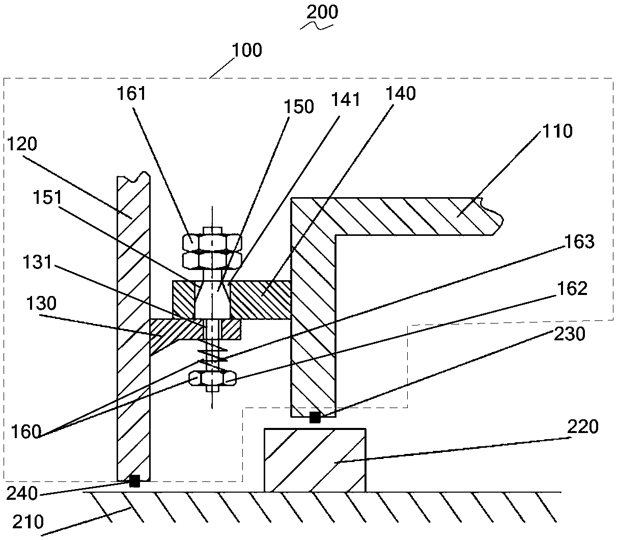
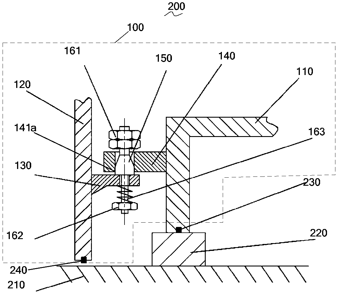
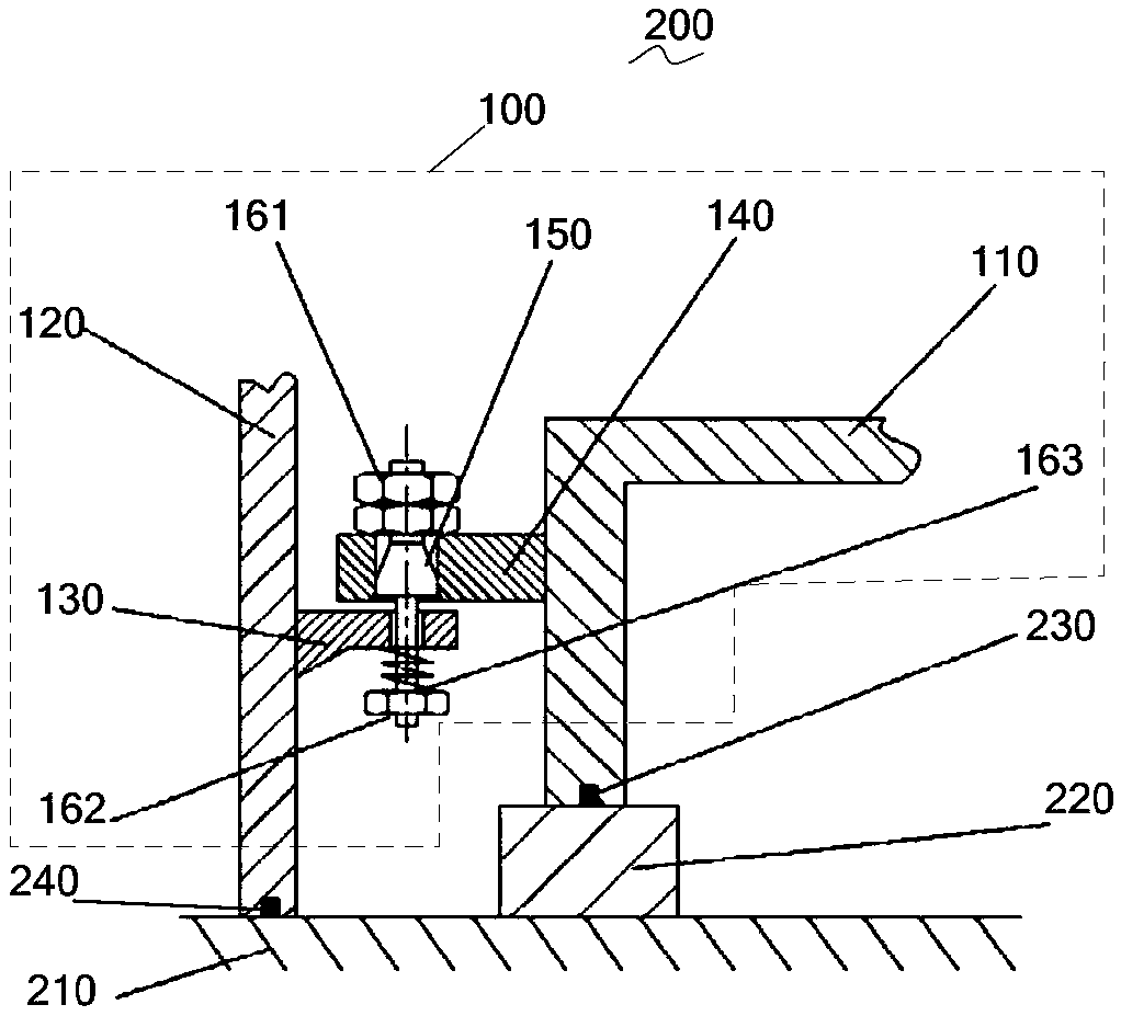
[0063] Such as Figure 1 to Figure 3 As shown, the first aspect of the present invention relates to a resonant cavity structure 100 , the resonant cavity structure 100 includes a resonant cavity body 110 , a protective shell 120 , a first support 130 , a second support 140 and a positioning member 150 . Wherein, the protective casing 120 is disposed outside the resonant cavity 110 . The first supporting member 130 is fixedly connected to the inner wall of the protective housing 120 . The second support 140 is fixedly connected to the outer wall of the resonant cavity 110, the second support 140 is located above the first support 130, and can overlap with the f...


PUM


Abstract

The invention discloses a resonant cavity structure and semiconductor processing equipment. The resonant cavity structure comprises a resonant cavity; a protective shell which covers the exterior of the resonant cavity; a first supporting piece fixedly connected with an inner wall of the protective shell; a second supporting piece which is fixedly connected with an outer wall of the resonant cavity body, is located above the first supporting piece and can be overlapped with the first supporting piece so as to be driven by the first supporting piece to ascend and descend; and a positioning piece which simultaneously penetrates through the first supporting piece and the second supporting piece along the lifting direction of the second supporting piece so as to position the first supporting piece and the second supporting piece. Therefore, in the cover opening process, the protective shell can be lifted to enable the first supporting piece to abut against the second supporting piece, so that the second supporting piece can be driven by the first supporting piece to ascend, the resonant cavity can be driven to be separated from a vacuum cavity, the rapid cover opening of the resonant cavity can be achieved, the cover opening efficiency of the resonant cavity is improved, and the cover opening time is shortened.

Description

technical field [0001] The invention relates to the technical field of semiconductor manufacturing, in particular to a resonant cavity structure and a semiconductor processing device. Background technique [0002] Generally, a surface wave plasma processing device includes a reaction chamber, a vacuum chamber, a resonant chamber and a protective shell. The resonant cavity is fixed on the top of the vacuum cavity by screws, the resonant cavity is covered with a protective shell, and the protective shell is connected with the reaction cavity. Elastic electromagnetic shielding rings are arranged between the resonant cavity and the vacuum cavity, and between the protective shell and the reaction cavity. [0003] However, in the above structure, every time the resonant cavity needs to be opened for maintenance, it is necessary to remove the protective case in advance, then remove the screws, and finally dismantle the resonant cavity. In addition, the space for screw removal is ...

Claims


Application Information

Patent Timeline
Patent Type & Authority Applications(China)
IPC IPC(8): H01J37/32
CPCH01J37/32431H01J37/32623
Inventor 段辰玥
Owner BEIJING NAURA MICROELECTRONICS EQUIP CO LTD
Why Eureka
Try Eureka