Chip precision film resistor array and manufacturing method thereof

A manufacturing method and precise technology, applied in the direction of resistance manufacturing, thin-film resistors, and resistors manufactured by photolithography, etc., can solve the problem that the inner wall of the through-hole of the exclusion substrate cannot be effectively covered

Active Publication Date: 2020-06-02
GUANGDONG FENGHUA ADVANCED TECH HLDG
View PDF6 Cites 3 Cited by
  • Summary
  • Abstract
  • Description
  • Claims
  • Application Information

AI Technical Summary

Problems solved by technology

[0004] The invention provides a chip-type precision thin-film exclusion and its manufacturing method to solve the technical problem that the film sticking method cannot effectively cover the inner wall of the through-hole of the

Method used


Image

  • Chip precision film resistor array and manufacturing method thereof
  • Chip precision film resistor array and manufacturing method thereof
  • Chip precision film resistor array and manufacturing method thereof

Examples


Embodiment

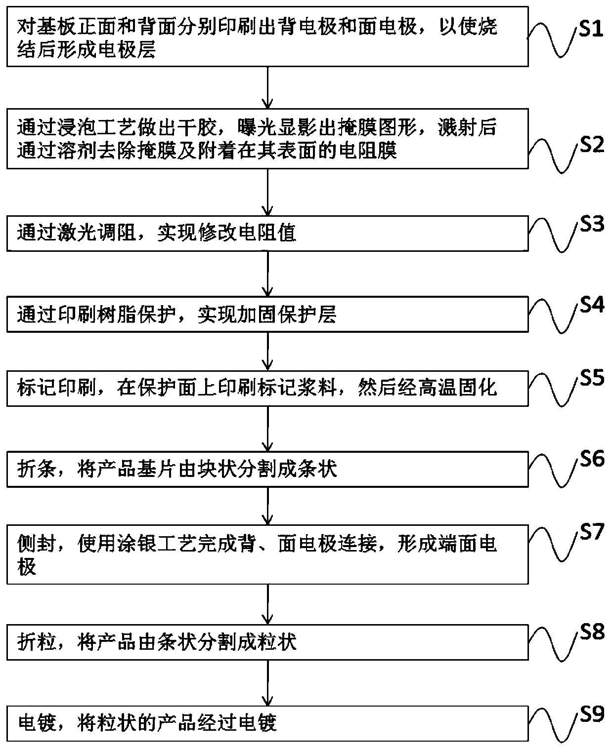
[0064] Please refer to Figure 7-Figure 8 , The specification model is 4R03, the target resistance is 10KΩ, the resistance precision control: ±0.5%, TCR: ±25ppm / ℃; it adopts alumina ceramic substrate.

[0065] The production process is as follows:

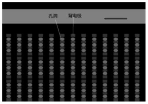
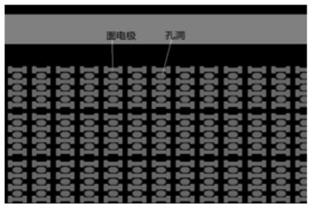
[0066] Step 1: Print the back and surface electrodes by printing, and form the electrode layer after sintering.

[0067] Step 2: Soak dry glue:

[0068] ① Put the product into the photoresist (phenolic resin) liquid, the thickness of the liquid film is 1.0 μm to 4.5 μm, the product moves up and down during soaking, so that the colloid completely covers the product hole, and the soaking time is 10 to 15 minutes.

[0069] ② After the colloid is covered, put the product in a drying oven and dry it at 100-150°C for 10 minutes. Obtain solid dry glue.

[0070] ③. Expose and develop the mask pattern, and after sputtering, remove the mask layer with a release agent to expose the resistor.

[0071] Step 3: Laser adjustment of resistanc...


PUM

PropertyMeasurementUnit
Film thicknessaaaaaaaaaa

Abstract

The invention discloses a manufacturing method of a chip precision film resistor array. The method comprises the following steps: S1, respectively printing a back electrode and a surface electrode onthe front surface and the back surface of a substrate so as to form an electrode layer after sintering; s2, preparing dry glue through a soaking process, exposing and developing a mask pattern, and removing a mask after sputtering to obtain a resistor body, and the dry glue completely covering the whole resistor array substrate; s3, modifying the resistance value through laser resistance trimming;s4, reinforcing a protection layer through printing resin protection; s5, carrying out mark printing, specifically, printing mark slurry on the protection face, and then carrying out high-temperaturecuring; s6, strip folding: cutting the product substrate into strips from blocks; s7, carrying out side sealing, and a back electrode to a surface electrode through a silver coating process to form an end surface electrode; s8, carrying out grain folding to divide the product into grains from a strip shape; and s9, electroplating the granular product. According to the invention, the film sputtering mask shielding layer is formed through the soaking process, so that the chip resistor array is thinned to film, and the resistor quality is improved.

Description

technical field [0001] The invention relates to the field of electronic component manufacturing, in particular to a chip-type precision thin film exclusion and a manufacturing method thereof. Background technique [0002] At this stage, chip exclusion is mostly thick film exclusion, and some use thin film exclusion, but thick film resistors have poor stability, while thin film resistors have higher precision and better stability, and are used in precision equipment; however, at this stage Thin-film exclusion components have a high demand for photolithography masks, and dry film lamination should be made according to the electrode and resistor margins. It is difficult to obtain a comprehensive sputtering pattern with ordinary film-attaching processes, and the through holes in the exclusion substrate are also difficult to obtain. Difficult to completely cover with film. Due to the design of the through-hole in the exclusion substrate, the thin-film sputtering mask shielding l...

Claims


Application Information

Patent Timeline
IPC IPC(8): H01C7/00H01C17/00H01C17/12H01C17/242H01C17/28
CPCH01C17/12H01C17/281H01C17/242H01C17/003H01C7/006
Inventor 杨泽明麦俊杨理强林瑞芬莫雪琼杨晓平
Owner GUANGDONG FENGHUA ADVANCED TECH HLDG
Why Eureka
Try Eureka