Methods of manufacturing a vertical memory device

A memory and charge storage technology, applied in semiconductor/solid-state device manufacturing, electrical solid-state devices, semiconductor devices, etc., and can solve problems such as the difficulty of semiconductor patterns

Pending Publication Date: 2020-06-02
SAMSUNG ELECTRONICS CO LTD
View PDF0 Cites 4 Cited by
  • Summary
  • Abstract
  • Description
  • Claims
  • Application Information

AI Technical Summary

Problems solved by technology

However, a semiconductor pattern may have a characteristic distribution such as a height distribution, and especially in a COP structure in which a circuit pattern may be formed u...

Method used


Image

  • Methods of manufacturing a vertical memory device
  • Methods of manufacturing a vertical memory device
  • Methods of manufacturing a vertical memory device

Examples


Embodiment Construction

[0013] It should be noted that aspects of the inventive concept described in one embodiment may be incorporated into a different embodiment, although not specifically described in this regard. That is, all embodiments and / or features of any embodiment may be combined in any manner and / or combination. These and other objects and / or aspects of the inventive concept are described in detail in the following specification. As used herein, the term "and / or" includes any and all combinations of one or more of the associated listed items. Expressions such as "at least one of," when preceding a list of elements, modify the entire list of elements and do not modify the individual elements of the list.

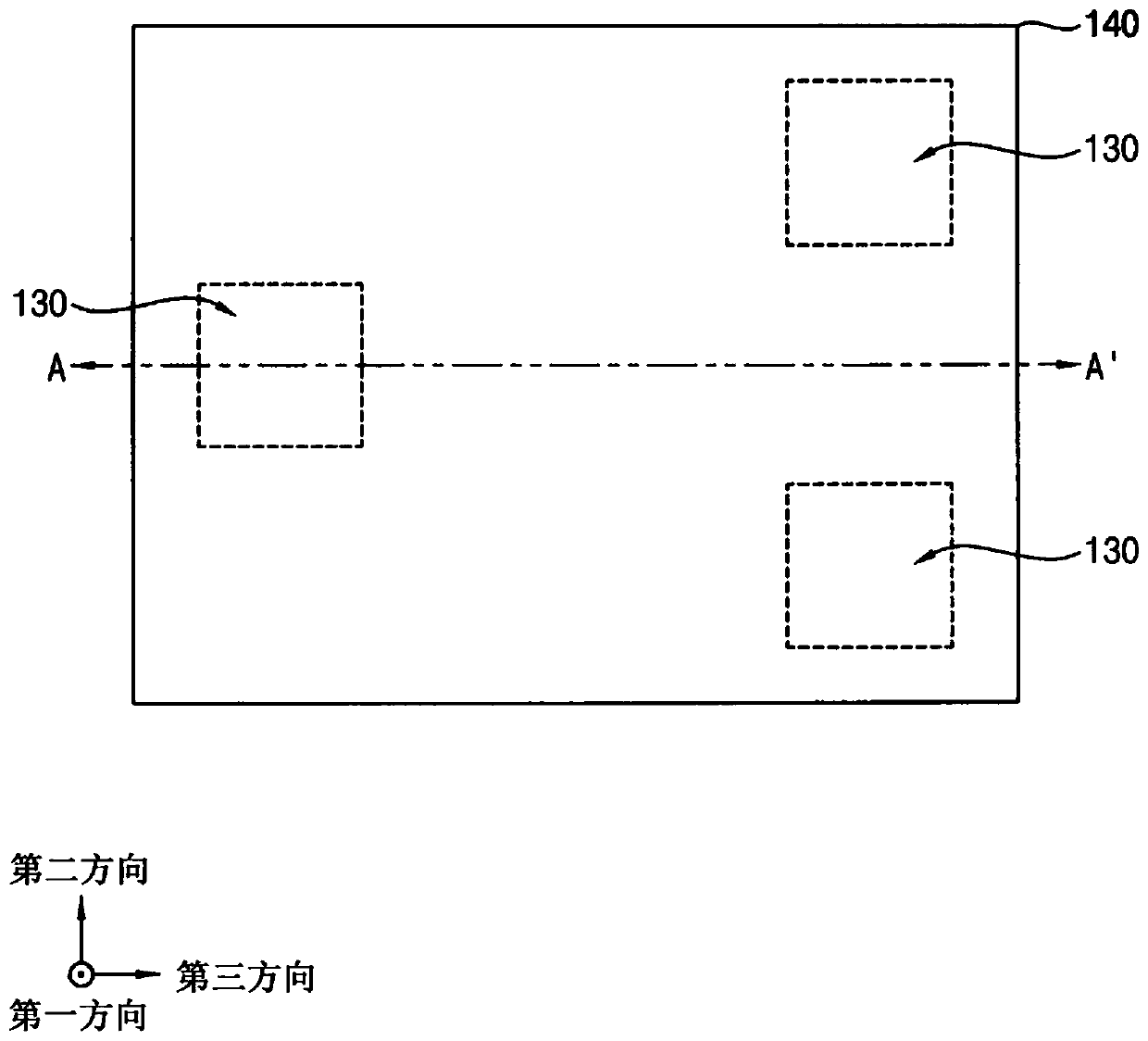
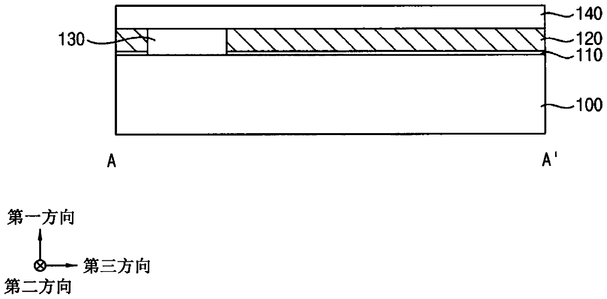
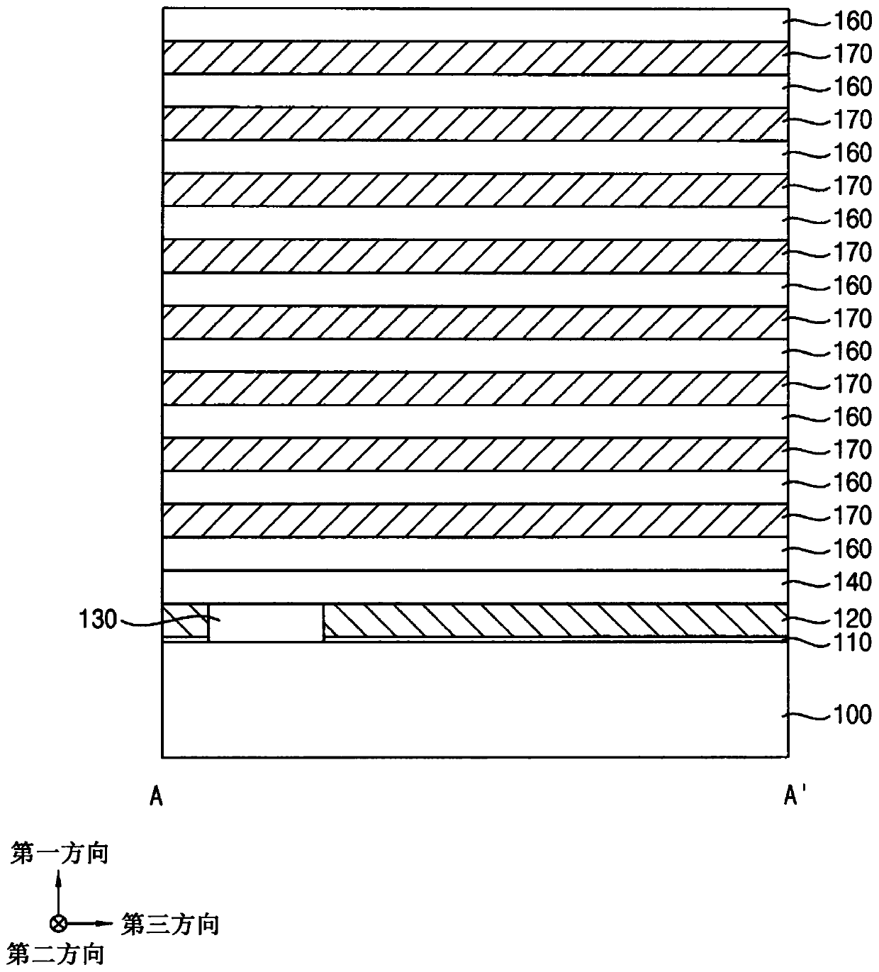
[0014] The above and other aspects and characteristics of a vertical memory device and a method of manufacturing the same according to example embodiments will become readily understood from the following detailed description with reference to the accompanying drawings. Hereinafter, a ...


PUM


Abstract

In a method of manufacturing a vertical memory device, a first sacrificial layer including a nitride is formed on a substrate. A mold including an insulation layer and a second sacrificial layer alternately and repeatedly stacked is formed on the first sacrificial layer. The insulation layer and the second sacrificial layer include a first oxide and a second oxide, respectively. A channel is formed by passing through the mold and the first sacrificial layer. An opening is formed by passing through the mold and the first sacrificial layer to expose an upper surface of the substrate. The first sacrificial layer is removed through the opening to form a first gap. A channel connecting pattern is formed to fill the first gap. The second sacrificial layer is replaced with a gate electrode.

Description

[0001] Cross References to Related Applications [0002] This application claims priority to Korean Patent Application No. 10-2018-0148338 filed with the Korean Intellectual Property Office (KIPO) on November 27, 2018, the contents of which are incorporated herein by reference in their entirety. technical field [0003] The inventive concept relates to a method of manufacturing a vertical memory device. Background technique [0004] To connect a channel to a substrate in a VNAND flash memory device, a channel hole may be formed through a mold including insulating layers and sacrificial layers alternately stacked on the substrate to expose the upper surface of the substrate. A selective epitaxial growth (SEG) process may be performed using the exposed upper surface of the substrate as a seed to form a semiconductor pattern, and a channel may be formed on the semiconductor pattern. However, a semiconductor pattern may have a characteristic distribution such as a height distri...

Claims


Application Information

Patent Timeline
IPC IPC(8): H01L27/11563H01L27/1157
CPCH10B43/00H10B43/35H01L21/31111H10B43/10H10B43/27H01L21/02164H01L21/32055H01L23/315H01L29/66825H01L29/66833H10B41/35H10B41/27
Inventor 金一宇安相基表炫坤金益秀朴嬉淑任智芸
Owner SAMSUNG ELECTRONICS CO LTD
Why Eureka
Try Eureka