

Display panel, manufacturing method thereof and display device
A display substrate, a part of the technology, applied in the direction of instruments, nonlinear optics, optics, etc., can solve the problems affecting the quality of the dark state picture, achieve the effect of improving light leakage and reducing the effect of birefringence
- Summary
- Abstract
- Description
- Claims
- Application Information
AI Technical Summary
Problems solved by technology
Method used
Image

Examples
Embodiment 1
[0054] Figure 3 to Figure 5 Shown is a schematic structural view of the display substrate in Example 1.
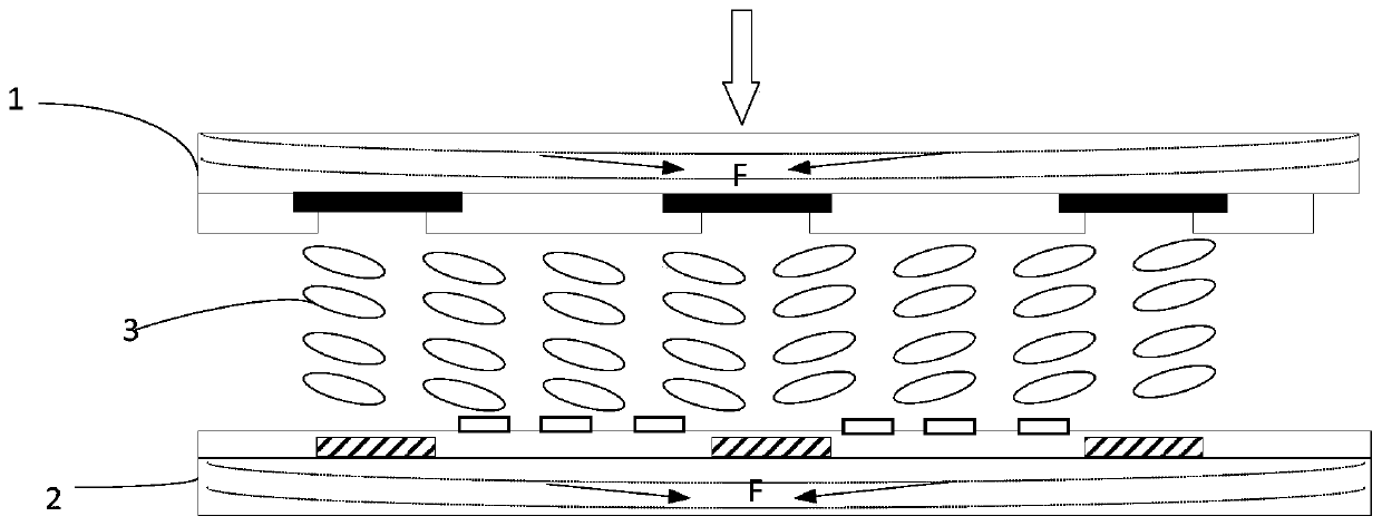
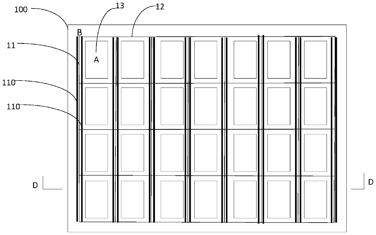
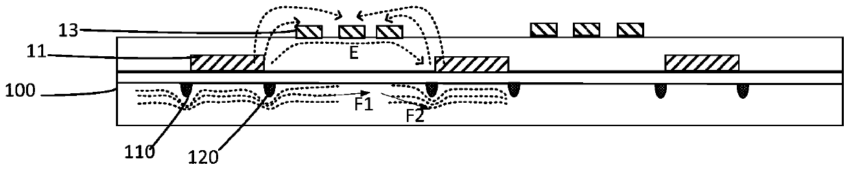
[0055] Such as Figure 2 to Figure 5 As shown, in this embodiment, the display substrate is an array substrate 10, and the array substrate 10 includes: a plurality of signal lines located on the first surface of the base substrate 100, and the signal lines include scanning lines and the data lines 11, a plurality of the scanning lines 12 and a plurality of the data lines 11 are intersected to define the pixel A, and the scanning lines 12 and the data lines 11 are located in the first area B; and, the pixel electrode 13 located in the pixel A; wherein, the strip-shaped groove 110 is arranged at a position corresponding to the data line 11 and is parallel to the data line 11; and / or, The strip groove 110 is disposed at a position corresponding to the scan line 12 and parallel to the scan line 12 .
[0056] In this embodiment, the display substrate is an array substrate 1...
Embodiment 2
[0070] Figure 6 to Figure 8 Shown is a schematic structural view of the display substrate in Example 2.
[0071] Such as figure 2 , Figure 6 to Figure 8 As shown, in this embodiment, the display substrate is a color filter substrate 20, which includes:
[0072]A black matrix formed on the first surface of the base substrate 100, the black matrix is located in the first region B, the black matrix includes a plurality of first portions 210 extending along a first direction and along A plurality of second parts extending in the second direction, a plurality of the first parts 210 and a plurality of the second parts are intersected to define the pixel A, wherein the first direction is the data on the array substrate 10 The extending direction of the line 11, the second direction is the extending direction of the scanning line 12 on the array substrate 10, or the first direction is the extending direction of the scanning line 12 on the array substrate 10, and the second dir...
PUM
 Abstract
Description
Claims
Application Information