Microelement transfer device

A transfer device, micro-component technology, applied in the direction of electrical components, electrical components, semiconductor devices, etc., can solve problems such as poor transfer effect

Active Publication Date: 2020-06-05
CHENGDU VISTAR OPTEOLECTRONICS CO LTD
View PDF5 Cites 5 Cited by
  • Summary
  • Abstract
  • Description
  • Claims
  • Application Information

AI Technical Summary

Problems solved by technology

[0003] The inventors of the present application found in the long-term research process that there are still problems such as poor transfer effect in the existing batch transfer process

Method used


Image

  • Microelement transfer device
  • Microelement transfer device
  • Microelement transfer device

Examples


Embodiment Construction

[0020] The following will clearly and completely describe the technical solutions in the embodiments of the present application with reference to the drawings in the embodiments of the present application. Obviously, the described embodiments are only some of the embodiments of the present application, not all of them. Based on the embodiments in this application, all other embodiments obtained by persons of ordinary skill in the art without making creative efforts belong to the scope of protection of this application.

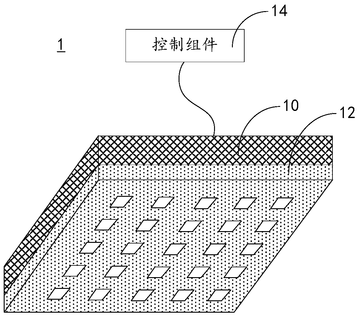
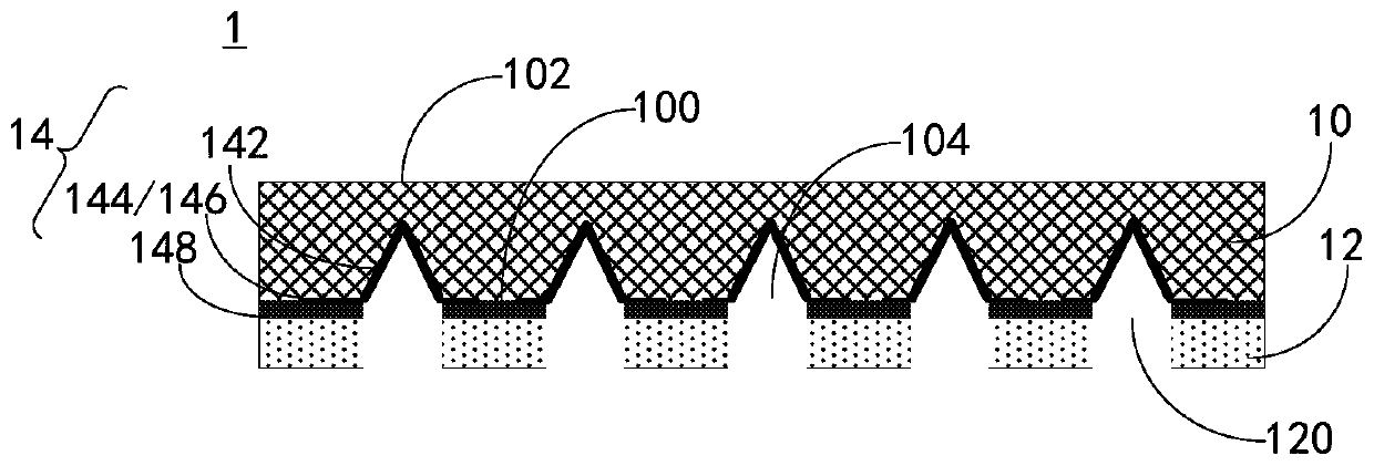
[0021] see Figure 1-Figure 2 , figure 1 It is a schematic structural diagram of an embodiment of the transfer device for micro components of the present application, figure 2 for figure 1 Schematic diagram of the cross-sectional structure of an embodiment of the transfer device. The transfer device 1 provided in the present application includes a transfer substrate 10 and a control component 14 .

[0022] Specifically, the material of the transfer substr...


PUM


Abstract

The invention discloses a microelement transfer device, which comprises a transfer substrate and a control assembly, wherein the transfer substrate comprises a first surface and a second surface, andthe first surface and the second surface are opposite to each other, and the first surface of the transfer substrate is provided with a plurality of first blind holes; and the control assembly is usedfor independently controlling the temperature of the gas in each first blind hole so as to control the first blind holes to adsorb or release the selected micro elements. By means of the mode, batchtransfer of the microelements can be achieved, and independent operation of each microelement can be further achieved in the batch transfer process.

Description

technical field [0001] The present application relates to the field of display technology, in particular to a transfer device and method for micro components. Background technique [0002] Micro-LED chips refer to micro-sized Micro-LED arrays integrated at high density on certain donor substrates (for example, donor wafers, etc.), and the size of Micro-LED chips is generally below 100 microns. During the manufacture of displays, it is generally necessary to batch transfer Micro-LED chips from a donor substrate to a target substrate. [0003] The inventors of the present application have found in the long-term research process that there are still problems such as poor transfer effect in the existing batch transfer process. Contents of the invention [0004] The technical problem mainly solved by this application is to provide a transfer device for micro components, which can realize batch transfer of micro components, and can further realize individual operation of each m...

Claims


Application Information

Patent Timeline
Patent Type & Authority Applications(China)
IPC IPC(8): H01L21/683H01L21/67H01L33/00
CPCH01L21/6838H01L21/67103H01L33/0095H01L21/67H01L21/683H01L33/00H01L21/67144H01L21/67721H01L21/67109H05K13/0408H01L25/0753
Inventor 王岩郭双孙建明
Owner CHENGDU VISTAR OPTEOLECTRONICS CO LTD
Why Eureka
Try Eureka