Display panel and display device
A display panel and array substrate technology, applied in semiconductor devices, electrical components, circuits, etc., can solve the problems of small color gamut and low overall brightness, achieve improved brightness, good display effect, and solve the effect of low overall display brightness
- Summary
- Abstract
- Description
- Claims
- Application Information
AI Technical Summary
Problems solved by technology
Method used
Image
Examples
Embodiment 1
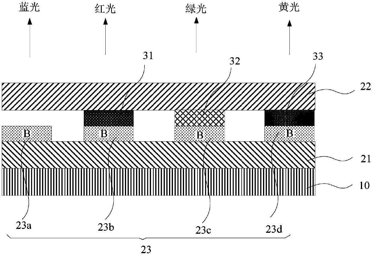
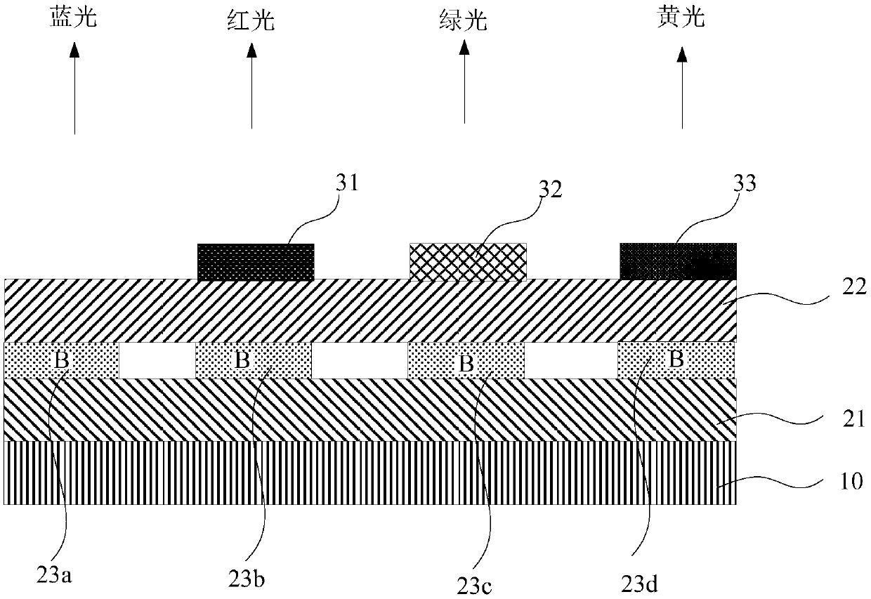
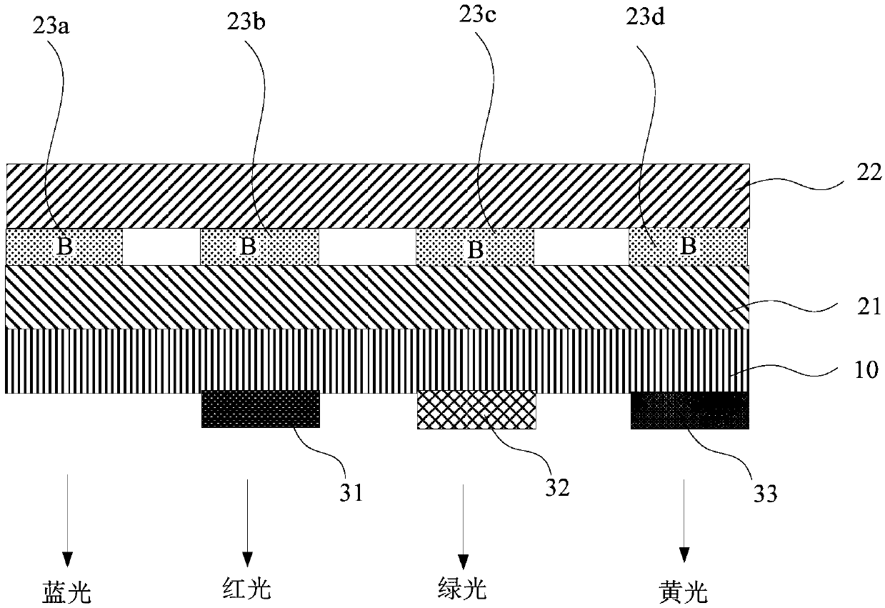
[0049] Figure 1A It is a schematic cross-sectional structure diagram of a display panel provided by Embodiment 1 of the present invention, Figure 1B Another schematic cross-sectional structure diagram of the display panel provided by Embodiment 1 of the present invention, Figure 1C Another schematic cross-sectional structure diagram of the display panel provided by Embodiment 1 of the present invention.
[0050] This embodiment provides a display panel, refer to Figures 1A-1C As shown, the display panel may specifically include: several light-emitting units arranged on the array substrate 10, each light-emitting unit includes a first electrode layer 21, an organic light-emitting layer 23 and a second electrode layer 22 stacked on the array substrate 10 in sequence , wherein, in this embodiment, in order to widen the color gamut and improve the display brightness, specifically, the organic light-emitting layer 23 includes: four sub-pixels, and the four sub-pixels can contr...
Embodiment 2
[0061] Figure 2A It is a schematic cross-sectional structure diagram of the display panel provided by Embodiment 2 of the present invention, Figure 2B Another schematic cross-sectional structure diagram of the display panel provided by Embodiment 2 of the present invention.
[0062] This embodiment provides a display panel, refer to Figure 2A As shown, the organic light-emitting layer 23 includes four sub-pixels, and there are three blue sub-pixels and one red sub-pixel 231 in the four sub-pixels, and the three blue sub-pixels are respectively blue sub-pixel 23a, blue sub-pixel 23c and the blue sub-pixel 23d, at the same time, in order to realize four-color display, a green quantum dot layer 32 is also provided on the light-emitting side of the organic light-emitting layer 23, that is, in this embodiment, the quantum dot layer includes: a green quantum dot layer 32 and a yellow quantum dot layer The quantum dot layer 33 has two quantum dot layers, wherein the green quantu...
Embodiment 3
[0071] image 3 It is a schematic cross-sectional structure diagram of a display panel provided by Embodiment 3 of the present invention.
[0072] In this embodiment, the organic light-emitting layer 23 includes four sub-pixels, and the four sub-pixels have two blue sub-pixels, one green sub-pixel 232 and one red sub-pixel 231, and the two blue sub-pixels are blue sub-pixels respectively. The pixel 23a and the blue sub-pixel 23d, at this time, only the yellow quantum dot layer 33 is provided on the light-emitting side of the organic light-emitting layer 23, wherein the yellow quantum dot layer 33 is used to convert the blue light emitted by the blue sub-pixel 23d into yellow The green sub-pixel 232 emits green light, and the red sub-pixel 231 emits red light, so that the light-emitting unit can generate four kinds of light: red, green, blue, yellow (RGBY).
[0073] Among them, in this embodiment, refer to image 3 As shown, the blue sub-pixel 23a emits blue light, the red su...
PUM
| Property | Measurement | Unit |
|---|---|---|
| thickness | aaaaa | aaaaa |
Abstract
Description
Claims
Application Information


