Chip burning method and system and computer readable storage medium

A programming method and chip technology, applied in computing, image data processing, instruments, etc., can solve problems such as inability to achieve mass production, incorrect correspondence between software serial numbers and chip location numbers, and cumbersome operations.

Inactive Publication Date: 2020-06-12
佛山普瑞威尔科技有限公司
View PDF0 Cites 0 Cited by
  • Summary
  • Abstract
  • Description
  • Claims
  • Application Information

AI Technical Summary

Problems solved by technology

First of all, the operator needs to correspond one-to-one with the software serial number of the chip and the position number of the chip on the circuit board when programming the chip. The operation is cumbersome and complicated, and only one chip can be burned at a time. The work efficiency is low and mass production cannot be achieved requirements; secondly, during the programming process, the operator is likely to make a wrong correspondence between the software serial number and the chip position number, resulting in defective products.

Method used


Image

  • Chip burning method and system and computer readable storage medium
  • Chip burning method and system and computer readable storage medium
  • Chip burning method and system and computer readable storage medium

Examples


Embodiment Construction

[0048] In order to understand the above-mentioned purpose, features and advantages of the present invention more clearly, the present invention will be further described in detail below in conjunction with the accompanying drawings and specific embodiments. It should be noted that, in the case of no conflict, the embodiments of the present application and the features in the embodiments can be combined with each other.

[0049] In the following description, many specific details are set forth in order to fully understand the present invention. However, the present invention can also be implemented in other ways different from those described here. Therefore, the protection scope of the present invention is not limited by the specific details disclosed below. EXAMPLE LIMITATIONS.

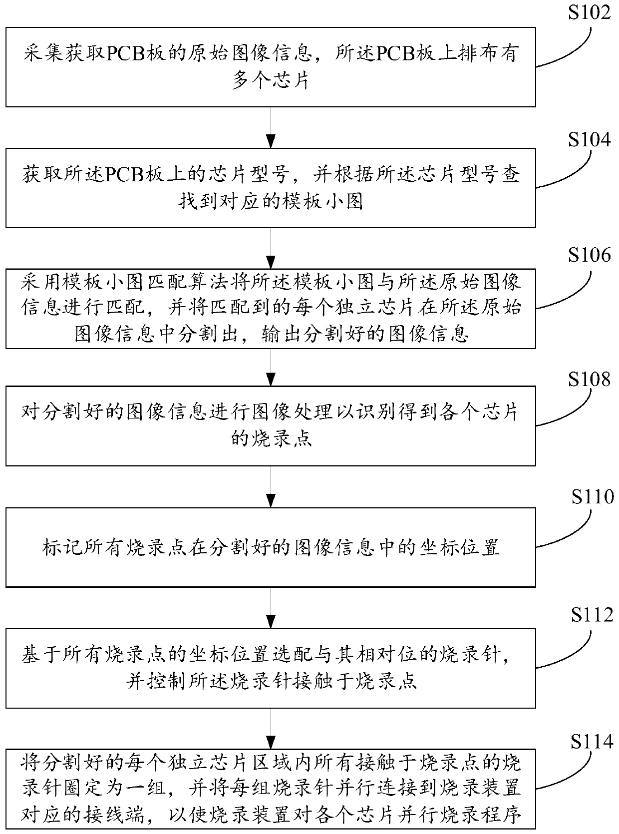
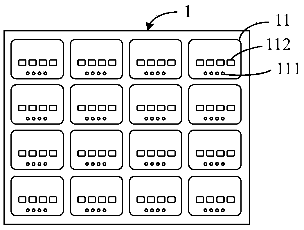
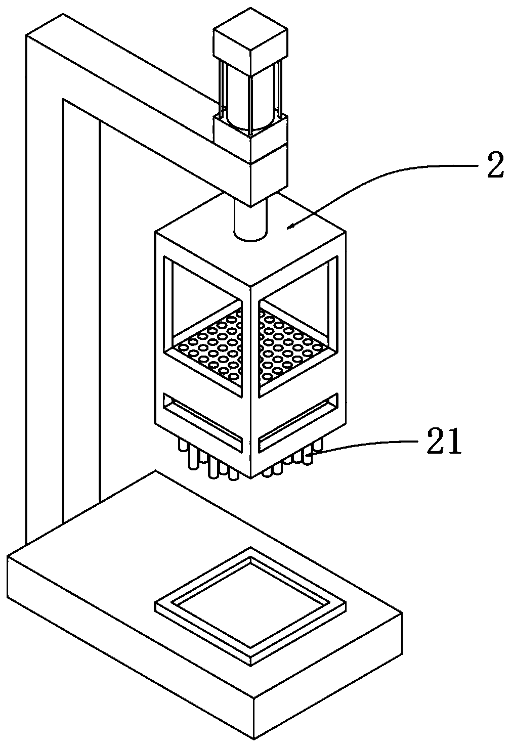
[0050] figure 1 A flow chart of a chip programming method of the present invention is shown.

[0051] Such as figure 1 As shown, the first aspect of the present invention proposes a chip programmi...


PUM


Abstract

The invention provides a chip burning method and system and a computer readable storage medium. The method comprises the steps that original image information of a PCB is acquired; acquiring a chip model and searching a corresponding template small graph according to the chip model; matching the template small graph with the original image information, and segmenting each matched independent chipin the original image information; performing image processing on the segmented image information to identify and obtain burning points of each chip; marking coordinate positions of all burning points; selecting burning needles corresponding to the burning points based on the coordinate positions of all the burning points, and controlling the burning needles to be in contact with the burning points; and delineating all the burning needles in contact with the burning points in each divided independent chip area into one group, and connecting each group of burning needles to the corresponding wiring end of the burning device in parallel so as to perform parallel program burning on each chip. According to the invention, a full-automatic chip burning process is realized, and the yield of chipburning is improved.

Description

technical field [0001] The invention relates to the technical field of chip programming, in particular to a chip programming method, system and computer-readable storage medium. Background technique [0002] At present, most electronic products on the market need to be controlled by chips, so it is necessary to program the chips. [0003] In the field of production of control equipment such as automotive ECU modules and air-conditioning control modules, it is necessary to burn the relevant control logic programs into the chip after the circuit is assembled. When programming the chip, it is necessary to fix the chip or related circuit board on the fixture and other instruments, and connect it with the programmer installed on the fixture, and then operate the host computer to control the programmer to burn the chip, and then burn the chip. After recording, remove the chip or circuit board from the fixture to complete the programming of a chip. [0004] The hardware structure...

Claims


Application Information

Patent Timeline
Patent Type & Authority Applications(China)
IPC IPC(8): G06T7/11G06T7/70
CPCG06T7/11G06T7/70G06T2207/10004
Inventor 周露露张凯
Owner 佛山普瑞威尔科技有限公司
Why Eureka
Try Eureka