
A debugging system and method for on-chip crash

A debugging system, electric crash technology, applied in the field of integrated circuits, can solve problems such as difficult chip debugging, high manpower and time costs

Active Publication Date: 2022-06-03
HUNAN GOKE MICROELECTRONICS
View PDF14 Cites 0 Cited by
  • Summary
  • Abstract
  • Description
  • Claims
  • Application Information

AI Technical Summary

Problems solved by technology

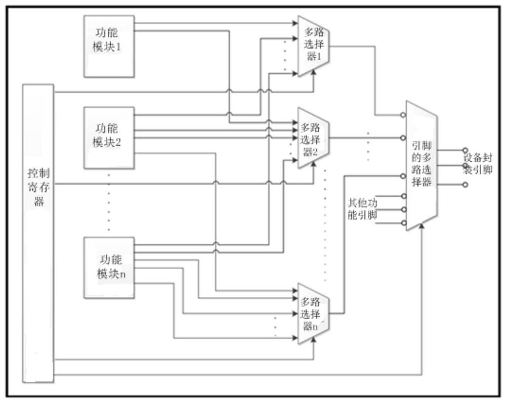
[0005] The number of internal signals observed in the first method can be set to multiple, but software cooperation configuration registers are required to implement debugging; the second method does not require software cooperation configuration registers compared to the first method, but specific pins need to be added to specify the chip Entering the debug mode, due to the limitation of the increased number of pins, it is difficult to truly implement chip debugging; the third method requires on-site debugging at the equipment provider factory, which is costly in manpower and time

Method used


Image

  • A debugging system and method for on-chip crash
  • A debugging system and method for on-chip crash
  • A debugging system and method for on-chip crash

Examples


Embodiment Construction

[0079] The debugging system of the on-chip electrical crash in the present invention is obviously different from the structure shown in FIG. 1, and it is not necessary to use a control

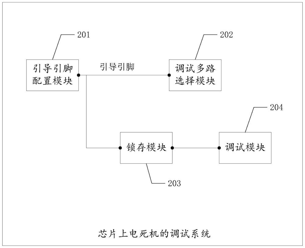
[0080] As shown in FIG. 2, an embodiment of the present invention provides a debugging system for an on-chip electrical crash, including:

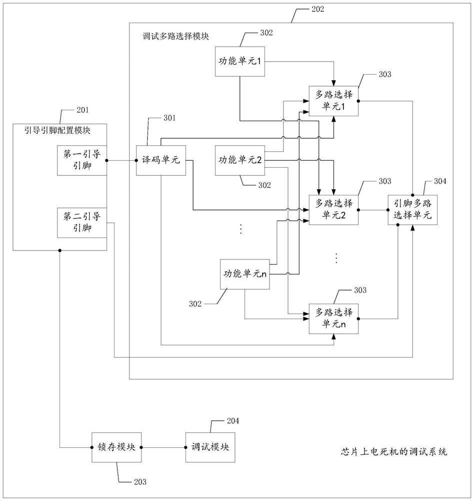
[0094] The multiplexing unit 303 is used to select the functional unit 302 according to the control signal;

[0097] Further, in conjunction with the embodiment shown in FIG. 3, as shown in FIG. 4, in some embodiments of the present invention, the debugging system

[0102] Further, in conjunction with the embodiment shown in FIG. 4, as shown in FIG. 5, in some embodiments of the present invention, the debugging system

[0107] The reset module 501 is also used to release the reset state when the chip is in the normal working mode.

[0109] Further, in conjunction with the embodiment shown in FIG. 5, as shown in FIG. 6, in some embodiments of the present inventi...


PUM


Abstract

The invention discloses a debugging system and method for on-chip power failure, which are used to solve the realizability of debugging when power on a chip crashes, and save the debugging cost. The debugging system includes: a boot pin configuration module, a debugging multiple selection module, a latch module and a debugging module; the boot pin configuration module is connected to the control terminal of the debugging multiple selection module and the latch module through the boot pin, and the latch module Connect with the debug module; the boot pin configuration module is used to configure the level information of the boot pin when the chip enters the debug mode when the power-on crash occurs, and controls the debug multi-channel selection module to establish a debug path; During the reset process, the level information of the boot pin is latched; the debugging module is used to obtain the level information of the boot pin from the latch module when the chip enters the normal working mode, and determine the debugging path according to the level information of the boot pin .

Description

A system and method for debugging an on-chip electrical crash technical field The present invention relates to the technical field of integrated circuits, particularly relate to a kind of debugging system and method of on-chip electrical crash Law. Background technique [0002] As the chip integrated logic becomes more and more complex and the cost becomes higher and higher, the more means of chip debugging (debug), the better. For example, the problem of power-on crash is fatal, but it is extremely difficult to debug because there are too few observation points. such as known For this purpose, the central processing unit (CPU) is powered on to start executing the Read-Only Memory (ROM) command, because the ROM has The instruction hangs up, causing the system chip to crash when powered on. There are debugging methods that cannot be deployed. Finally, trace back through the chip code And automatic test equipment (Automatic Test Equipment, ATE) test to locate the bug...

Claims


Application Information

Patent Timeline
Patent Type & Authority Patents(China)
IPC IPC(8): G01R31/317
CPCG01R31/31705Y02D10/00
Inventor 亓磊
Owner HUNAN GOKE MICROELECTRONICS
Learn More