Method for measuring secondary electron emission yield of medium

A technology of secondary electron emission and secondary electrons, applied in measuring devices, material analysis using wave/particle radiation, instruments, etc., can solve problems such as poor relative accuracy, achieve accurate measurement results, good scientific research and market application prospects Effect

Active Publication Date: 2020-06-19
XIAN INSTITUE OF SPACE RADIO TECH
View PDF7 Cites 2 Cited by
  • Summary
  • Abstract
  • Description
  • Claims
  • Application Information

AI Technical Summary

Problems solved by technology

The bias voltage neutralization method is to change the bias voltage, the default is weak positive charging to neutralize the negative charging state, the relative accuracy is poor, and it has strong limitations on the output test of the low energy section

Method used


Image

  • Method for measuring secondary electron emission yield of medium
  • Method for measuring secondary electron emission yield of medium
  • Method for measuring secondary electron emission yield of medium

Examples


Embodiment Construction

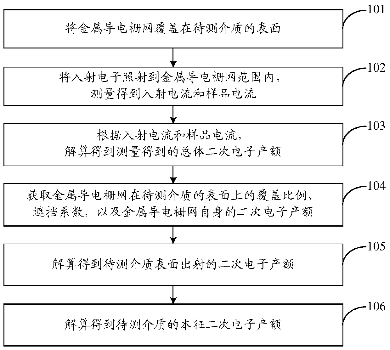
[0041] In order to make the object, technical solution and advantages of the present invention clearer, the embodiments disclosed in the present invention will be further described in detail below in conjunction with the accompanying drawings.

[0042] Such as figure 1 , in this embodiment, the method for measuring the secondary electron emission yield of the medium includes:

[0043] Step 101, covering the surface of the medium to be tested with a metal conductive grid.

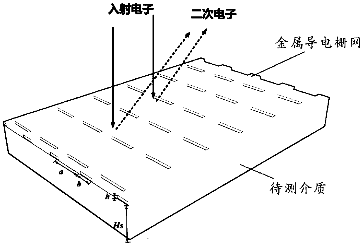
[0044] In this example, if figure 2 , the metal conductive grid is: a grid structure obtained by processing metal good conductor materials, covering the surface of the medium to be tested, so that most of the charges on the surface of the medium to be tested are guided away through the metal conductive grid.

[0045] Note: The width of the metal conductive grid is b, the thickness is h, the grid width is a, and the thickness of the medium to be tested is Hs; then there are: a≤0.5Hs, and a≤200um; b≤0.2a; h...


PUM


Abstract

The invention discloses a method for measuring the secondary electron emission yield of a medium. The method comprises the following steps: covering the surface of a medium to be measured with a metalconductive grid mesh; irradiating incident electrons into the range of the metal conductive grid mesh, and carrying out measurement to obtain incident current and sample current; according to the incident current and the sample current, obtaining the total secondary electron yield obtained through measurement by calculation; obtaining the coverage ratio of the metal conductive grid mesh on the surface of the to-be-measured medium, the shielding coefficient of the metal conductive grid mesh on emergent electrons on the surface of the to-be-measured medium at the lower layer, and the secondaryelectron yield of the metal conductive grid mesh; resolving to obtain the yield of secondary electrons emitted from the surface of the medium to be measured; and calculating to obtain the intrinsic secondary electron yield of the to-be-measured medium. The method does not need a high-precision neutralizing means, can be universally used for common metal secondary electron yield testing equipment,is accurate in measurement result, is not limited by the thickness of the sample, and can better adapt to a low-energy end.

Description

technical field [0001] The invention belongs to the technical field of secondary electron emission, in particular to a method for measuring the secondary electron emission yield of a medium. Background technique [0002] Secondary electron emission, also known as secondary electron multiplication, refers to the phenomenon that electrons or other particles with certain energy emit electrons from the surface of solid materials when they irradiate the surface of solid materials. When the part is at 10 -3 Pa or lower pressure, under the condition of high power, it is easy to cause resonance discharge phenomenon due to secondary electron emission, which is called micro-discharge effect. The mechanism of secondary electron generation can be briefly summarized as follows: when electrons are incident on the surface of a material with a certain energy, they scatter multiple times with atoms or molecules in the material, and part of the electrons are elastically scattered with surfac...

Claims


Application Information

Patent Timeline
Patent Type & Authority Applications(China)
IPC IPC(8): G01N23/2251
CPCG01N23/2251G01N2223/07
Inventor 封国宝王琪杨晶苗光辉谢桂柏何鋆崔万照
Owner XIAN INSTITUE OF SPACE RADIO TECH
Why Eureka
Try Eureka