Non-adhesive seed crystal type tantalum crucible and crystal growing method

A tantalum crucible, non-adhesive technology, applied in the field of semiconductor manufacturing equipment and processes, to achieve the effects of high melting point, saving the use of glue, excellent chemical corrosion resistance and thermal shock performance

Inactive Publication Date: 2020-06-26
哈尔滨科友半导体产业装备与技术研究院有限公司
View PDF5 Cites 7 Cited by
  • Summary
  • Abstract
  • Description
  • Claims
  • Application Information

AI Technical Summary

Problems solved by technology

[0011] The invention solves the defect problem existing in the current sticking seed crystal type aluminum nitride growth device

Method used


Image

  • Non-adhesive seed crystal type tantalum crucible and crystal growing method
  • Non-adhesive seed crystal type tantalum crucible and crystal growing method
  • Non-adhesive seed crystal type tantalum crucible and crystal growing method

Examples


specific Embodiment approach 2

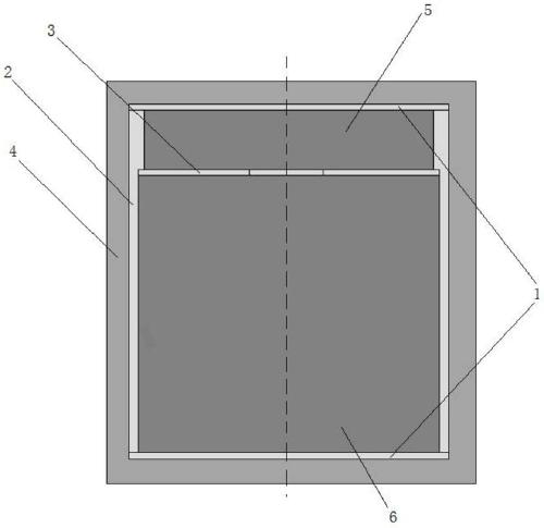
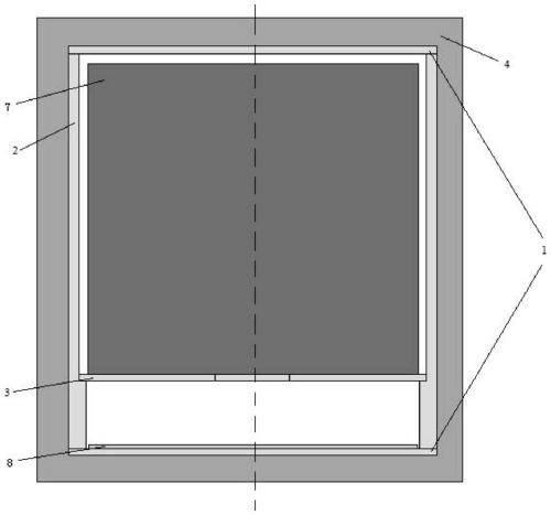
[0046] Specific implementation mode two: combination Figure 1-Figure 4 This embodiment will be described. In the non-adhesive seed crystal tantalum crucible of this embodiment, the inner diameter difference between the two ends of the tantalum crucible cylinder 2 is within the range of 1.8 mm to 2 mm.

specific Embodiment approach 3

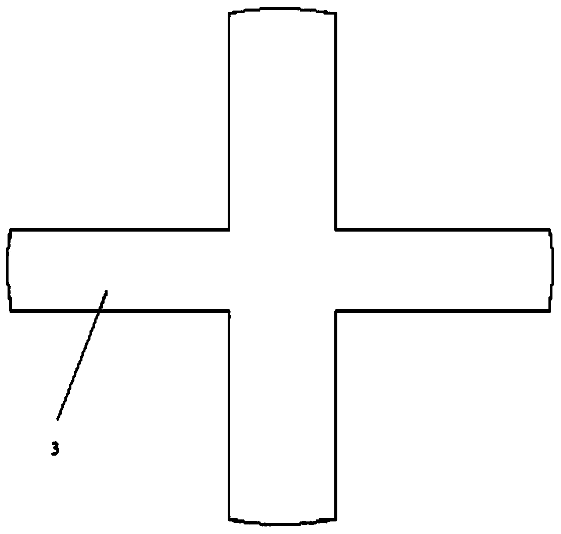
[0047] Specific implementation mode three: combination Figure 1-Figure 4 This embodiment will be described. In the non-adhesive seed crystal tantalum crucible of this embodiment, the thickness of the cross tantalum sheet 3 is within the range of 1 mm to 1.5 mm.

[0048] Specific implementation mode four: combination Figure 1-Figure 4 Describe this embodiment, a non-adhesive seed crystal tantalum crucible of this embodiment, the four edges of the cross tantalum sheet 3 are arc-shaped, and the arcs of the four arcs are the same as the arcs of the inner surface of the tantalum crucible cylinder 2 Consistently, the length of the cross tantalum sheet 3 is slightly smaller than the inner diameter of the end of the tantalum crucible cylinder 2 with a larger inner diameter, and the difference is within 0.6mm-0.8mm.

[0049] Specific implementation mode five: combination Figure 1-Figure 4 To illustrate this embodiment, a method for growing crystals in a non-adhesive seed crystal t...


PUM

PropertyMeasurementUnit
thicknessaaaaaaaaaa

Abstract

The invention discloses a design and application method of a non-adhesive seed crystal type tantalum crucible, and belongs to the technical field of semiconductor manufacturing and processes. According to the method, the defects existing in current preparation of an aluminum nitride single crystal by using a physical vapor transport method are overcome. The tantalum crucible comprises tantalum wafers, a tantalum crucible cylinder, a cross-shaped tantalum sheet, a graphite heat preservation structure, a raw material placement area, a crystal growth area, an aluminum nitride raw material and a seed crystal. The tantalum wafers cover two ends of the tantalum crucible cylinder, the tantalum crucible cylinder is placed in the graphite heat preservation device, the inner diameters of two ends ofthe tantalum crucible cylinder are different, wherein the inner side surface of the tantalum crucible cylinder is step-shaped, the cross-shaped tantalum sheet is transversely erected in the tantalumcrucible cylinder, an area formed between the cross-shaped tantalum sheet and the upper tantalum wafer is a crystal growth area, an area formed between the cross-shaped tantalum sheet and the lower tantalum wafer is a raw material placement area, an aluminum nitride raw material is placed in the raw material placement area, and a seed crystal is placed in the crystal growth area. The non-adhesiveseed crystal type tantalum crucible is simple in structure, and the situation that seed crystal needs to be fixed to the crucible cover through glue in the past is replaced.

Description

technical field [0001] The invention relates to a non-adhesive seed crystal tantalum crucible and a method for growing crystals, belonging to the technical field of semiconductor manufacturing devices and processes. Background technique [0002] Aluminum nitride is one of the third-generation semiconductor materials. It has excellent characteristics such as high band gap, high breakdown field strength, high thermal conductivity, high saturation electron drift rate, and strong chemical stability. Power, anti-radiation devices and deep ultraviolet photoelectric devices have broad application prospects. [0003] At present, only the physical vapor transport method is used to prepare aluminum nitride single crystals. The basic process of the physical vapor transport method is that in a specific temperature field, the solid powder used as the growth raw material decomposes and sublimates to generate gas phase components. Driven by the axial temperature gradient, the gas phase co...

Claims


Application Information

Patent Timeline
Patent Type & Authority Applications(China)
IPC IPC(8): C30B29/40C30B23/00
CPCC30B23/00C30B29/403
Inventor 不公告发明人
Owner 哈尔滨科友半导体产业装备与技术研究院有限公司
Why Eureka
Try Eureka