

Trench isolation
A technology for isolating trenches and conductors, which is applied in semiconductor/solid-state device manufacturing, semiconductor devices, electrical components, etc., and can solve problems such as undesired floating and short circuits.
- Summary
- Abstract
- Description
- Claims
- Application Information
AI Technical Summary
Problems solved by technology
Method used
Image

Examples
Embodiment Construction
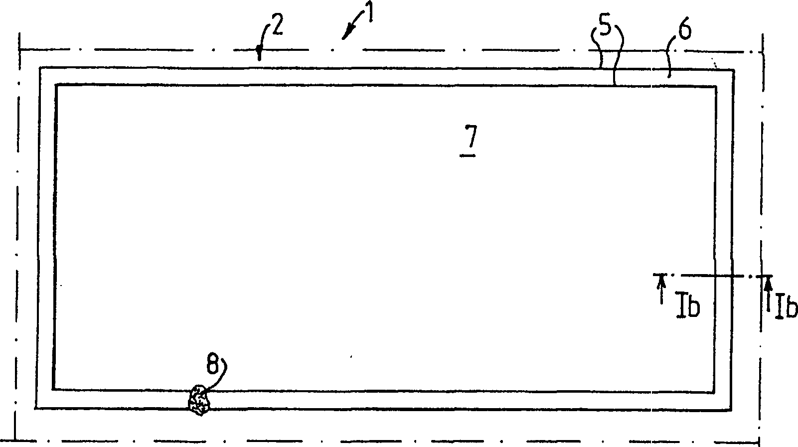
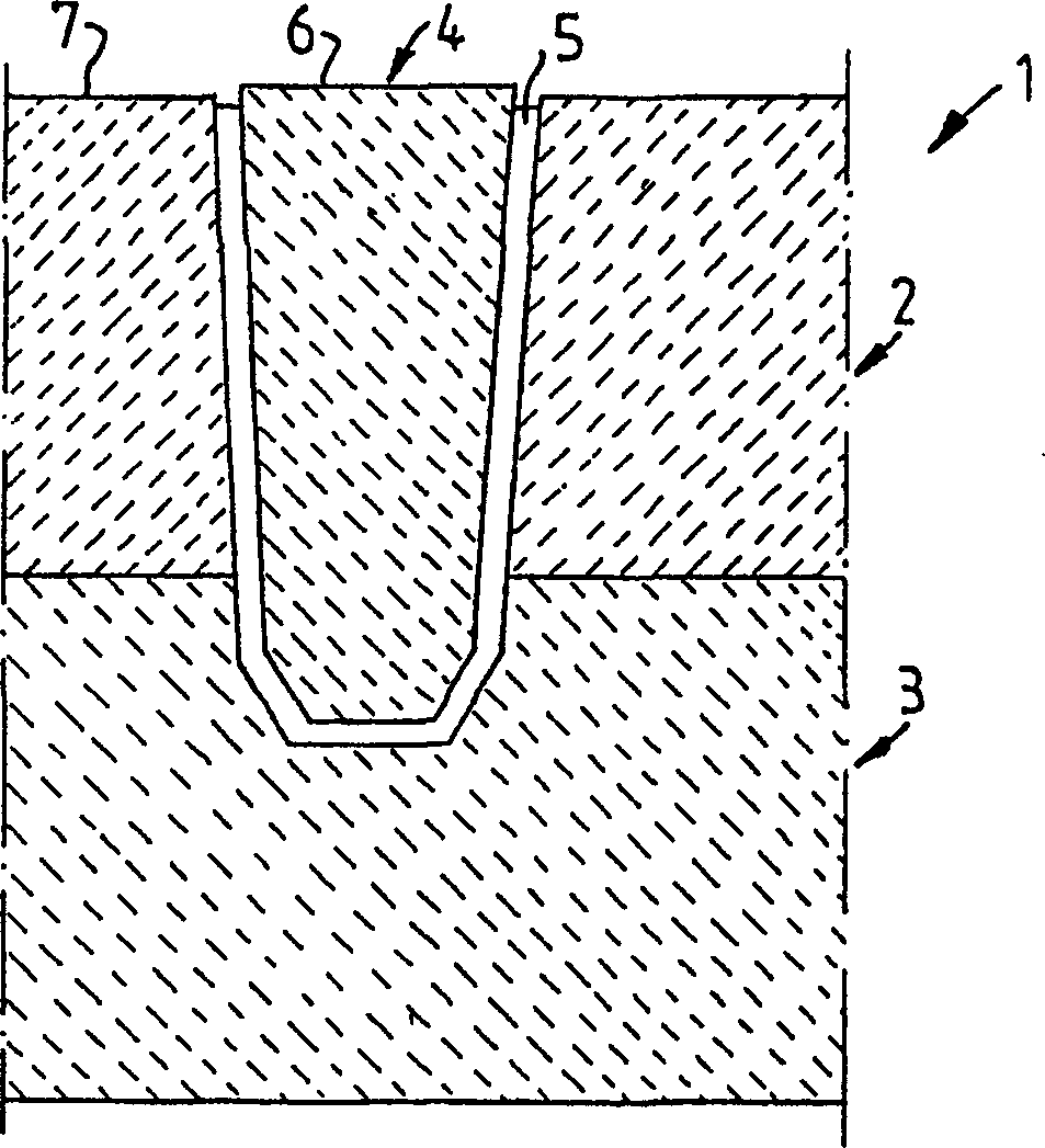
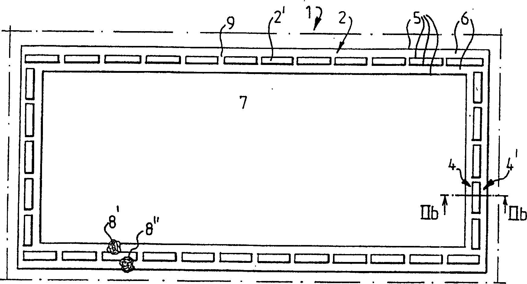
[0018] In the prior art trench structure shown in FIG. 1 , a wafer 1 for making a semiconductor device has a layer of doped silicon (such as n-type silicon) covered on an inversion-doped silicon layer 3 (p-type silicon here). doped silicon) layer 2. The wafer has grooves 4 which are continuous or closed loops. Groove 4 has a U-shaped cross-section extending from the upper surface of wafer 1 through layer 2 to layer 3 . The groove 4 has insulating walls 5 made of eg silicon oxide and a polysilicon filler 6 between the groove walls 5 . Groove 4 extends along the boundary between n-type doped silicon island 7 and the remainder of n-type doped silicon 2 and isolates silicon island 7 from the remainder of n-type doped silicon 2 . The silicon island 7 can be used to fabricate one or more components (not shown), such as resistors, capacitors, diodes, transistors and other bipolar components. In the case of conductive foreign particles or impurities in the material (to simplify the...
PUM
 Abstract
Description
Claims
Application Information