

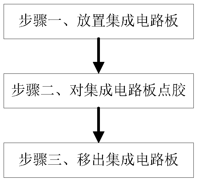
Integrated circuit board manufacturing method
An integrated circuit board and manufacturing method technology, which is applied in the manufacturing of circuits, electrical components, semiconductor/solid-state devices, etc., can solve the problems of too many contests, the inability to keep the surface of the integrated circuit board parallel, and the reduction of the sticking effect of the patch components. Guaranteed accuracy
- Summary
- Abstract
- Description
- Claims
- Application Information
AI Technical Summary
Problems solved by technology
Method used
Image

Examples
Embodiment Construction
[0034] The embodiments of the present invention will be described in detail below with reference to the accompanying drawings, but the present invention can be implemented in many different ways defined and covered by the claims.
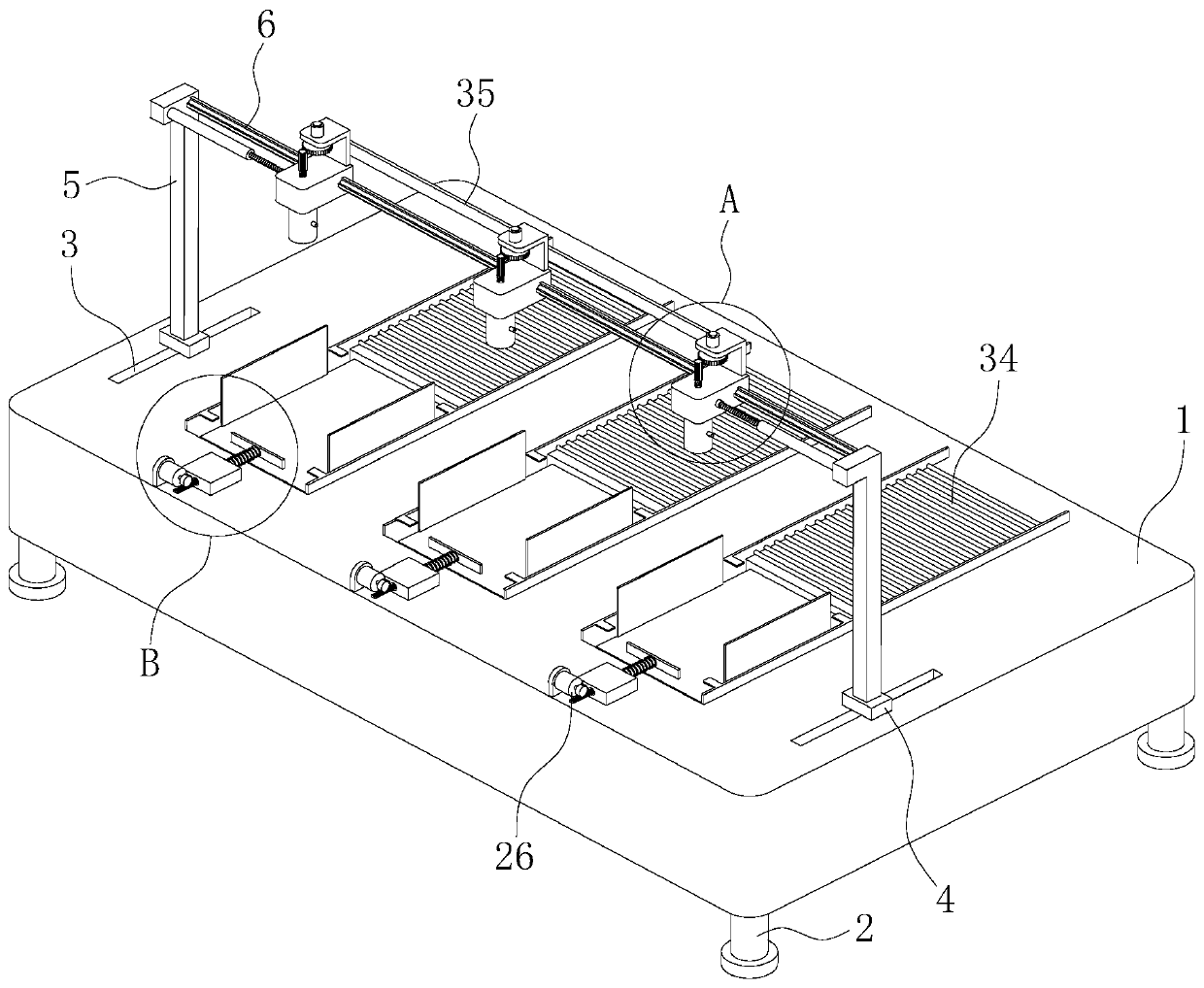
[0035] Such as Figure 2 to Figure 7 As shown, this embodiment provides an integrated circuit board manufacturing and processing device, including a base 1 , the top surface of the base 1 is horizontal, and the bottom surface is vertically fixed with support legs 2 . The upper surface of the base 1 is provided with two mutually parallel chute 3, and the chute 3 is slidingly fitted with an electric slider 4, and the top of the electric slider 4 is vertically fixed with a support column 5, and the support columns 5 are fixed horizontally. Guide rod 6 is installed.
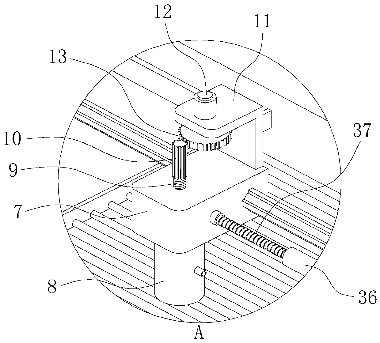
[0036] On the guide rod 6, a mounting block 7 is slidably installed, and the upper and lower surfaces of the mounting block 7 are in a horizontal state and the lower surface of the mounti...
PUM
 Abstract
Description
Claims
Application Information