Display panel, manufacturing method thereof and display device

A technology for a display panel and a substrate is applied in the fields of display devices and display panels, and can solve the problems of increased production cost of display panels, difficult connection of initialized signal line patterns, limited layout space of display panels, etc.

Active Publication Date: 2020-07-31
BOE TECH GRP CO LTD
View PDF10 Cites 15 Cited by
  • Summary
  • Abstract
  • Description
  • Claims
  • Application Information

AI Technical Summary

Problems solved by technology

[0004] The object of the present invention is to provide a display panel and its manufacturing method, and a display device, which are used to solve the problem of the limited layout space of the d

Method used


Image

  • Display panel, manufacturing method thereof and display device
  • Display panel, manufacturing method thereof and display device
  • Display panel, manufacturing method thereof and display device

Examples


Embodiment Construction

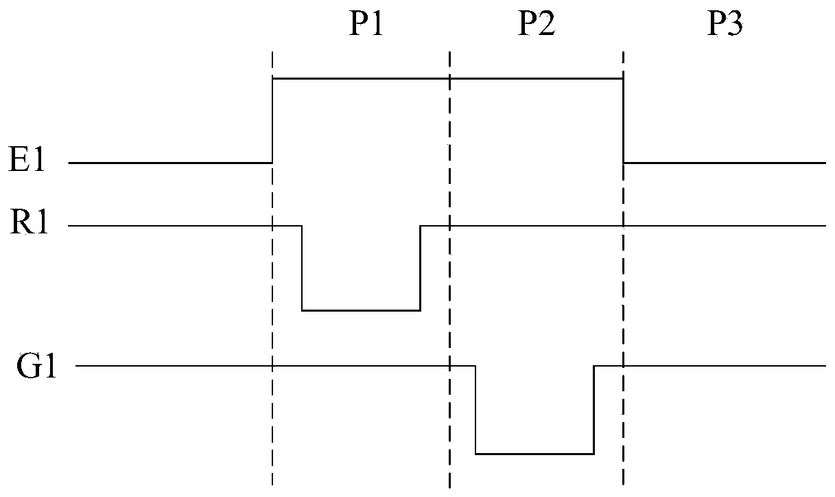
[0076] In order to further illustrate the display panel, the manufacturing method thereof, and the display device provided by the embodiments of the present invention, a detailed description will be given below in conjunction with the accompanying drawings.

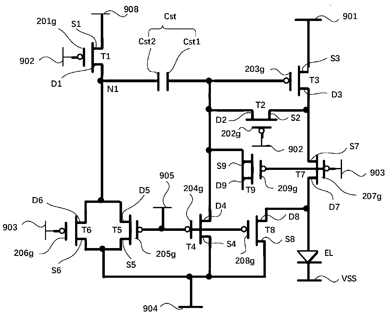
[0077] see Figure 1 to Figure 5 , an embodiment of the present invention provides a display panel, including: a substrate, and an initialization signal line layer and an anode layer sequentially stacked on the substrate along a direction away from the substrate; and a plurality of sub-pixels distributed in an array Area;

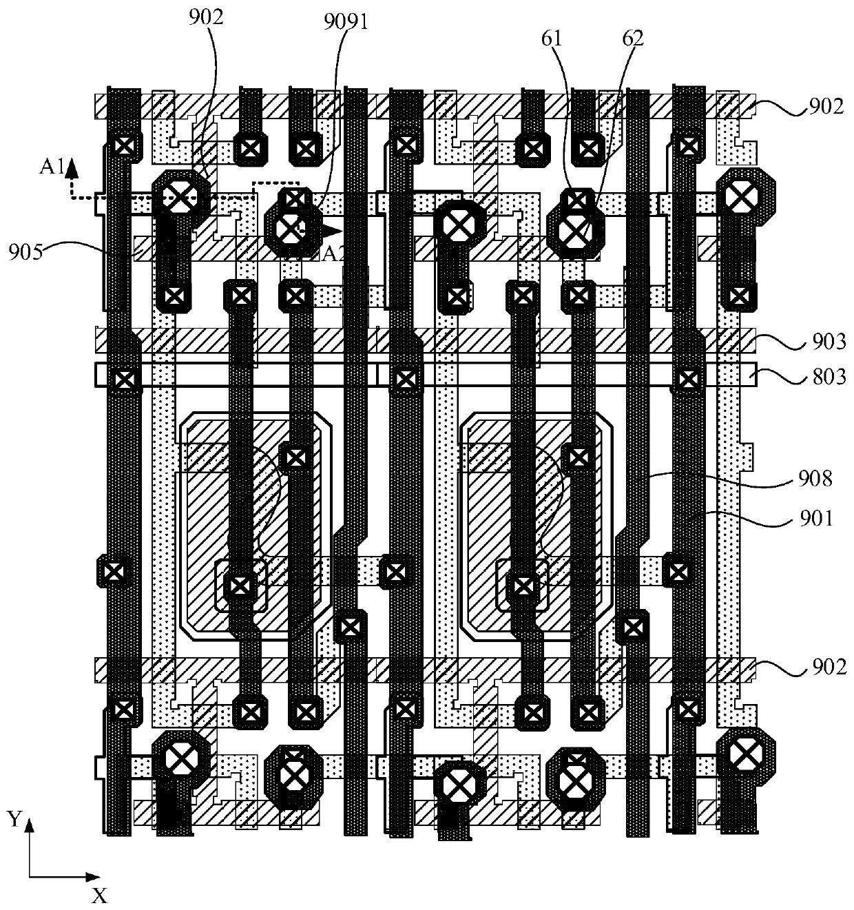
[0078] Such as image 3 , Figure 4 and Figure 7 As shown, the initialization signal line layer includes an initialization signal line pattern 904 arranged in each of the sub-pixel regions;

[0079] Such as Figure 5 As shown, the anode layer includes a plurality of anode patterns 906 corresponding to the plurality of sub-pixel regions one by one, the plurality of anode patterns 906 are arranged ...


PUM


Abstract

The invention provides a display panel, a manufacturing method thereof and a display device, relates to the technical field of display, and aims to solve the problem that the production cost of the display panel is increased due to the fact that initialization signal line graphs in the same row are not easy to connect together due to the fact that the layout space of the display panel is limited.An initialization signal line layer in the display panel comprises initialization signal line patterns arranged in all sub-pixel areas. The first auxiliary signal line layer comprises a plurality of first auxiliary signal line patterns in one-to-one correspondence with the plurality of sub-pixel regions, and the first auxiliary signal line patterns are coupled with the initialization signal line patterns in the corresponding sub-pixel regions; at least part of the first auxiliary signal line patterns extend in the first direction, and in the same row of sub-pixel areas, the first auxiliary signal line patterns corresponding to the sub-pixel areas are sequentially coupled. The display panel provided by the invention is used for displaying pictures.

Description

technical field [0001] The present invention relates to the field of display technology, in particular to a display panel, a manufacturing method thereof, and a display device. Background technique [0002] Active-matrix organic light-emitting diode (English: Active-matrix organic light-emitting diode, abbreviated: AMOLED) display panel is widely used in various fields due to its advantages of self-illumination, low power consumption, and fast response speed. The AMOLED display panel includes a sub-pixel driving circuit and a light-emitting unit, and the sub-pixel driving circuit drives the corresponding light-emitting unit to emit light, so as to realize the display function of the display panel. [0003] However, as the resolution of the display panel becomes higher and higher, the layout space in the display panel becomes smaller and smaller. When laying out the initialization signal line pattern for providing the initialization signal for the sub-pixel driving circuit, t...

Claims


Application Information

Patent Timeline
IPC IPC(8): H01L27/32G09G3/3225
CPCG09G3/3225H10K59/131H10K59/1201G09G3/3233G09G2300/0426G09G2300/0842G09G2300/0819H10K59/351G09G2300/0465H10K71/00H10K59/1213H10K59/1216
Inventor 陈义鹏皇甫鲁江刘利宾
Owner BOE TECH GRP CO LTD
Why Eureka
Try Eureka